BusyEng
Newbie level 6
Hi folks,
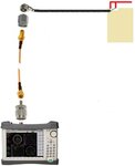
I am very new to the field of RF measurement and need some help to correctly set up the VNA, interfacing cables, connectors and DUT to make a correct measurement. Using my Anritsu MS2024B VNA, I would like to measure the impedance and Return Loss of a 2.4GHz printed antenna (such as a loop, Meander, or Inverted F antenna). These antennas are very small and are printed on very small circuit boards too. There is no room for a SMA connector to be placed on the board. Therefore, my only option is to solder a very tiny coaxial cable to the feeding points of the antenna on the PCB. I use something like Hirose U.FL-2LP-04N2-A-(200) cable that has two UFL connectors on its ends. I cut the cable on one end and come up with a cable that has a UFL connector only on one side. I solder the center wire of the free side of the cable to the feeding point of the antenna on the PCB. I also remove few millimeters of the plastic jacket to expose the shield and solder the shield to the edge of the GND plane somewhere close to the feeding point of the antenna. Then I use a UFL to SMA adapter to connect the tiny coaxial cable to a RG316 cable (such as Amphenol 135110-01-24.00). I attach a SMA to N adapter on the MS2024B to connect the other side of the RG-316 cable to the MS2024B port. The picture here shows the connections that I just explained.
My Questions here are:
1) I cannot use a regular SMA RF terminator or calibration kit here. How can I do the calibration? Can I just keep the end of the UFL cable open and consider it as Open then solder the center wire to shield and consider it as the short for calibration purpose?
2) What can I use as the 50Ω load for calibration is such application? can I just use a 50Ω 0402 SMD resistor?
3) How should l I setup the VNA for calibration? For example, How do I define the Calibration coefficients in this configuration for User-Defined Port setup? (how to find the values of Short Offset, Open Offset, Open C0, Open C1, Open C2, Open C3 variables needed for User-Defined Port Setup?)
Thanks
I am very new to the field of RF measurement and need some help to correctly set up the VNA, interfacing cables, connectors and DUT to make a correct measurement. Using my Anritsu MS2024B VNA, I would like to measure the impedance and Return Loss of a 2.4GHz printed antenna (such as a loop, Meander, or Inverted F antenna). These antennas are very small and are printed on very small circuit boards too. There is no room for a SMA connector to be placed on the board. Therefore, my only option is to solder a very tiny coaxial cable to the feeding points of the antenna on the PCB. I use something like Hirose U.FL-2LP-04N2-A-(200) cable that has two UFL connectors on its ends. I cut the cable on one end and come up with a cable that has a UFL connector only on one side. I solder the center wire of the free side of the cable to the feeding point of the antenna on the PCB. I also remove few millimeters of the plastic jacket to expose the shield and solder the shield to the edge of the GND plane somewhere close to the feeding point of the antenna. Then I use a UFL to SMA adapter to connect the tiny coaxial cable to a RG316 cable (such as Amphenol 135110-01-24.00). I attach a SMA to N adapter on the MS2024B to connect the other side of the RG-316 cable to the MS2024B port. The picture here shows the connections that I just explained.

My Questions here are:
1) I cannot use a regular SMA RF terminator or calibration kit here. How can I do the calibration? Can I just keep the end of the UFL cable open and consider it as Open then solder the center wire to shield and consider it as the short for calibration purpose?
2) What can I use as the 50Ω load for calibration is such application? can I just use a 50Ω 0402 SMD resistor?
3) How should l I setup the VNA for calibration? For example, How do I define the Calibration coefficients in this configuration for User-Defined Port setup? (how to find the values of Short Offset, Open Offset, Open C0, Open C1, Open C2, Open C3 variables needed for User-Defined Port Setup?)
Thanks