Continue to Site

Welcome to EDAboard.com

Welcome to our site! EDAboard.com is an international Electronics Discussion Forum focused on EDA software, circuits, schematics, books, theory, papers, asic, pld, 8051, DSP, Network, RF, Analog Design, PCB, Service Manuals... and a whole lot more! To participate you need to register. Registration is free. Click here to register now.

[SOLVED] OPAMP simple circuit problem

Status
Not open for further replies.
Phew, thanks - all this pole talk is really quite vague to me...
Don't let the terminology confuse you, it's actually pretty simple. Here's a couple of simple RC filters, a low pass and a high pass, with their responses:


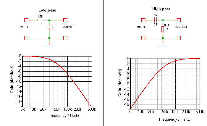
In both cases we say there's a pole at 50KHz, because that's the frequency above (or below) which the gain rolls down. When the response curves the other way (upwards), it's called a zero.

According to your example (0.5MHz --> 5MHz), shouldn't the added criteria be:
5) no added poles below fug_total*10
What I meant was that, all else being equal, fug_total is 0.5MHz with the LM358, but it's 5MHz with the NE5532. So changing the opamp changes the fug.

Which brings me to the main point I'm missing: How to find out where those added poles are? For example, how did you calculated the added pole due to Cgd?
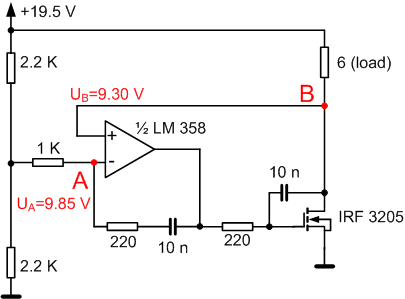
The filter below has the same response as the MOSFET gain stage with the values I suggested: 330R and 10nF, with Cdg = 500pF.


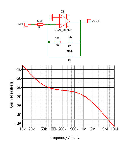
There's a pole at 1MHz from 330R and 500pF, and a zero at 50KHz from 330R and (10nF + 500pF).

Oh, and BTW - as I said, it works very well even for 3 MOSFETs but with the values of 220R and 100nF (I came to this empirically, but would like some approximate formula to have some generic solution for this topology), and I was testing on NE5532.
220R with 3 MOSFETs puts the pole at the same frequency as 330R with 2 MOSFETs. Your choice of 100nF is much more conservative than my 10nF, pushing the zero down to about... um, 7KHz? (without reaching for the calculator). Nothing wrong with that.
 
"Which brings me to the main point I'm missing: How to find out where those added poles are? For example, how did you calculated the added pole due to Cgd?"

Assuming Cgd is 500pF (which can be seen by looking at the IRF3205's datasheet; look in Fig.5 at the plot for Crss—this is Cgd, the MOSFET's internal capacitance from gate to drain), the added pole occurs at 1/(2*pi*330Ω*500pF)=1MHz. Remembering the series RC we considered earlier, but replacing R=330Ω and C=10nF, we now place a capacitor in parallel to these of value 500pF. The impedance of this combo is very high at low frequencies and decreases until it reaches 50kHz, at which point it levels off at 330Ω, and then above 1MHz it falls again.

You can visualize this easily using LTspice. Here's a graph of the impedance, and the circuit that produced it:

screen-capture-6.png

I'm feeding the network a current of amplitude 1, so the voltage across the network represents its impedance (V=IZ; for I=1, V=Z). As you can see, with Cgd absent the impedance remains resistive at high frequencies (red), which was the intended operation. However, with the large Cgd introduced, the impedance becomes capacitive again above ~1MHz (orange), which brings the phase down and causes instability if the unity gain frequency occurs above it.

Looking at the orange graph, we notice three distinct regions. Starting from the left the impedance is falling, indicating a capacitive impedance (since for a capacitor, Z=1/sC). The fall is at 20dB/dec, which also indicates a single-pole rolloff (the pole occurred at zero frequency). Whenever you have a pole, it is accompanied by a falling gain—20dB/dec per pole. At 50kHz a zero is introduced by the resistor. If there weren't any poles, the zero would actually cause a 20dB/dec rise, but since there was already a pole it simply cancels out the fall, resulting in a level region above 50kHz. At 1MHz a second pole occurs, causing the impedance to fall again.

Doing the math explicitly, we have a parallel combination of (1/sCgd) // (R+1/sC). This translates to:
\[Z=\frac{1}{sCgd+sC/(sCR+1)}\].
\[=\frac{sCR+1}{sCgd(sCR+1)+sC}\].
\[=\frac{sCR+1}{s[sCgdCR+Cgd+C]}\].
\[=\frac{sCR+1}{\frac{s}{C+Cgd}[s\frac{CCgd}{C+Cgd}R+1]}\].
\[=\frac{sCR+1}{\frac{s}{C+Cgd}[s(C//Cgd)R+1]}\].
This equation expresses the impedance as a function of frequency, s (where s is in general a complex number, but we usually substitute jω for sinusoidal signals; I prefer to write s because it saves space). Occurrences of s in the numerator cause "zeros" in the frequency response (here, you can see that the impedance goes to zero if s=-1/CR), while occurrences in the denominator cause "poles" in the response (you can see the impedance goes to infinity if s=0 or if s=-1/(C//Cgd)R). For sinusoidal signals we won't actually see zeros and infinities here, but we will still see something distinctive happen—we'll see a change in the slope. We have a pole at ω=0 causing the impedance to fall from the start; then we have a zero at ω=1/CR causing the impedance to level off, and finally another pole at ω=1/(C//Cgd)R causing the impedance to fall again. Intuitively, if I'm graphing something in the numerator (such as y=x) then it should go up as I traverse the horizontal axis, and if I graph something in the denominator (such as y=1/x) it should go down. The more terms in the numerator (y=x² or x³), the faster it rises, and the more terms in the denominator (y=1/x² or 1/x³), the faster it falls. Same thing happens here.

One thing to notice is that for the second pole at ω=1/(C//Cgd)R, C»Cgd (10nF»500pF). In "parallel" combinations, the smaller value dominates, so we can approximate the pole frequency to ω=1/CgdR. This is in line with what was stated earlier, indicating that we didn't actually need to do all this math, although it's useful for building our confidence.


Stepping back for a bit, this all comes into play by affecting the MOSFET's gain. Its voltage gain in this configuration is (again, approximately) Zfeedback/Zdrive. Since Zdrive is a resistor of 6.8kΩ, this stage behaves as an integrator below 50kHz, transitions to an amplifier of gain 0.05, and then behaves like an integrator again above 1MHz. The gain curve will roughly follow the feedback impedance curve. The new R and C value don't guarantee stability when you add fifty more MOSFETs on, but it should have good margin with one.

As crutschow recommended, it's a good idea to simulate the circuit. You can find a model of the IRF3205 from International Rectifier (hopefully its model is suitable; you can compare it to the datasheet for a double-check. Instead of reading the values, you can build simulations that try to mimic the datasheet graphs, and then see how close they are—this saves you the headache of trying to figure out what every single simulation parameter is). When simulating the circuit, this is what I get:

screen-capture-3.png

Obviously, I couldn't be bothered with figuring out how to get a nice symbol working so I added the MOSFET's subcircuit with a SPICE line. With any luck, this MOSFET amplifier shouldn't make the global loop unstable. Plug in a model for an op-amp, and evaluate the loop gain. This is what I get with an ideal, single-pole opamp with a 1MHz unity gain frequency (some call it the gain-bandwidth product, GBWP, or GBW):

screen-capture-4.png

This simulation shows about 45 degrees of phase margin at 59kHz, which most people consider acceptable. Going through the exercise of simulating sections and subsections, and tweaking values to see how things change, can really be enlightening. Simulations can also help catch issues you didn't realize would be there.
 
Last edited:
Thank you both for your time and knowledge sharing. I think I'm now a bit more clearer on what those poles actually are - I'm only sorry I don't have more points to give away :)...

Regarding the suggestions on using simulation - a few years back, when I had more time to play with electronics, I tried some simulation software (the last one was Electronic Workbench, as far as I remember), but I didn't really had much luck with those - there was either too steep learning curve, or the results didn't agree with actual measurements. There were also various glitches, for example, when abrupt changes were simulated. Finally I just got frustrated with those, and used experimental board/actual measurement instead. I realize advantages of the simulation, but they do require time investment to properly use (otherwise, you aren't sure is its the software limitation/bug, or your own), and time is unfortunately something I lack at right now... So now, I prefer analytic results when possible (read - not to hard), and I think you just helped me on that regarding this particular topology.
On that note, may we now conclude that the stability will (probably :)) be achieved if, in addition to previously stated conditions, the following is also satisfied:

5. 1/(2*pi*R*Cgd)>fug_total (assuming Cgd<<C, where Cgd is gate-to-drain capacitance of the used mosfet)
 

"Regarding the suggestions on using simulation - a few years back, when I had more time to play with electronics, I tried some simulation software ... but I didn't really had much luck with those ... There were also various glitches, for example, when abrupt changes were simulated ... they do require time investment to properly use (otherwise, you aren't sure is its the software limitation/bug, or your own), and time is unfortunately something I lack at right now..."

Sure thing. But when you get a chance, I would recommend learning LTspice. There's a multitude of reasons for this suggestion:
1. LTspice has relatively simple operation, meaning you can get up to speed quickly.
2. The software has a large user base —*this means that you can easily find support. Numerous books have been written describing its operation, and there's even a Yahoo! group devoted to it.
3. The program's help file is actually helpful. When in doubt, hit F1 and you'll have tons of information at your fingertips.
4. The SPICE solver was written with the express intent of simulating switching regulators, so it usually doesn't have the trouble converging that other solvers do.

And of course, the normal reasons for learning any SPICE simulator:
5. It helps build your intuition for electrical networks and feedback loops and helps for catching circuit bugs before they happen.
6. When bugs do happen, simulation can often help you figure out where your understanding was incomplete.
7. You can use it to simulate non-electrical systems, such as mechanical, thermal, and fluid systems.

Cheers
 
Thanks for the recommendation, I'll be sure to try it!
 

Hello again - I'm really sorry to keep harping on this subject again, but I build a PCB and the problem reappeared (though it worked nicely on the breadboard). After pulling my hear out trying to debug PCB layout, testing and replacing components etc., I finally narrowed the problem down to the value of the load. It seems that stability is influenced by the load as well (in my original post its 1K, which didn't change until I actually built and started using the damn thing).
The circuit performs quite OK for 1K load. However, if the load used is 10 ohms (hence parallel mosfets - the load can be as low as 5 Ohms), the stability is once again disrupted (I get about 0.5V difference between opamp inputs). Before pestering everybody again, I tried all kinds of R,C combinations, googled for opamp instability and tried some of the proposed solutions, but no matter what I tried, the problem persisted - thus this post.

Once again, I'm sorry to raise the issue again, but If you would have a bit more patience with me on this problem I would be very grateful - what to do if load is not 1K but 10 ohms?
 

seeker13,

Are you sure it's the load, and not the number of MOSFETs, that is driving it unstable? As long as the load has a greater impedance than the MOSFET's rs (= 1/gm), then treating it as an inverting amplifier is fair. At 1A, simulation shows rs at 77mOhm, which is well below the load's resistance. So we should be safe. Perhaps the input voltage to the op-amp isn't actually 12V?

Closing the loop, simulation shows that it should be stable, virtually regardless of load. The fact that the ringing decays quickly indicates good stability:

seeker13.png

To view and edit the simulation circuit which produced this plot, see the attached "seeker13.txt" file. Download it, change the file extension to ".asc", and then open it in LTspice (If you don't have LTspice yet, it can be downloaded for free from Linear's website). You can zoom in and out using the mouse wheel, you can edit components and text by right-clicking, and you can run a simulation by clicking the running man at the top.
 

Attachments

  • seeker13.txt
    3.7 KB · Views: 50
  • Like
Reactions: seeker13 and js

    js

    Points: 2
    Helpful Answer Positive Rating

    seeker13

    Points: 2
    Helpful Answer Positive Rating
Hi ZekeR, thanks for responding again.
The - input of opamp is actually about 12.5V. The only thing different than circuit I originally posted is that the circuit supply voltage is, of course, not from ideal voltage source. In case this matters, I measured approximately 24.7V, but it varies slightly (it's a rectified and filtered transformer output). AC component is between 50mV and 100mV. When load is reduced to about 6 ohms, I measure supply voltage drop from 24.7V to about 20V. This happens for a single MOSFET and LM358 (which previously produced best results).

Unfortunately, this then seems to be one of those cases when simulation doesn't agree with the real world I guess. As I said, I just don't seem to have much luck with the simulators :(.
Anyway, would you happen to have any other idea how to try stabilizing this circuit, other then RC circuit between G and D?
 
Last edited:

Pretty much calculations for an essentially simple circuit. I would use a slightly different compensation scheme as a first try, which has the advantage of not causing oscillations when compensating too strong, as the present one does.

It's a series RC from OP output back to non-inverting input. In addition, you may want to speed-up the gate voltage divider by a parallel capacitor to the upper R.

P.S.: I apologize for creating confusion.

I meant inverting input.
 
Last edited:
  • Like
Reactions: LvW

    LvW

    Points: 2
    Helpful Answer Positive Rating
Hi FvM - I'm afraid series RC between opamp +input and output doesn't help either (I tried various combinations of C=4n7/10n/100n/0.1u and R=10 ohm/100 Ohm/330 Ohm/1K). Did you have some other value combination in mind?
Btw, parallel C (1u/100n) to upper 6K8 seem to make things worse. Also, using your proposal in combination with godfreyl's further increases the voltage between + and - opamp inputs.
Any other idea?
 

Hi seeker13,

I think FvM meant to create a feedback network to the op-amp's inverting input, such as in this circuit. (see attached, and convert to .asc to open in LTspice). This way, the op-amp's loop gain needn't be considered because its feedback is derived from a small local loop.

-- Edit --

The circuit shown works just as well if the 220Ohm resistors are replaced with 2.2kOhm resistors. This would permit your entire circuit to use the same resistor value. The stability can be improved further by increasing C2's value.
 

Attachments

  • seeker13_2.txt
    4 KB · Views: 56
Last edited:
  • Like
Reactions: FvM

    FvM

    Points: 2
    Helpful Answer Positive Rating
Right, thank you for the correction.

For maximum speed, you won't place additional C's across MOSFET drain-gate and set the compensation element as small as possible.
 

Sorry to report that this also doesn't improve things...Just to make a quick checkpoint, I'm posting the currently tested circuit, along with the DC measurements of opamp input voltages. In the interest of simplicity I'm only using 1 MOSFET, but it gets really hot, so I didn't have time to wait for the voltages to stabilize - in short, take them as an approximate values.

3975770900_1369303142.gif
 

Okay. Let's try a really conservative compensation approach: Change the 220Ohm resistors to 2.2kOhm and change the 1kOhm resistor to 100kOhm. This is going to reduce the bandwidth quite substantially and hopefully have large stability margins. If it works, you can improve the DC accuracy (by several millivolts) by introducing a 100kOhm resistor between point B and the op-amp's non-inverting input.
 

The circuit shown in post #33 has a stable loop gain and seems to behave orderly in a simulation.
 

zekeR - nope, the things even got worse in this case (difference between A and B went up to 1V).

FvM - I know, but so did the one before it. IMHO, the reasons for this apparent disparity between reality and simulation is limited to some of the following categories:

(1) I made mistake in circuit assembly - so no actual disparity, just a good old human error.
I think the probability for this the case is quite low, and this is why. This is the first thing I suspected. So I checked and rechecked - since this is quite simple "skeleton" test circuit, I think after a few rechecks its unlikely that I'm missing something (just in case, I disassembled and reassembled the circuit from scratch). In addition, the circuit works OK for a lighter load (1K), which additionally reduces the chances I miss-assembled something (so that it doesn't work only for larger loads).

(2) MOSFET or opamp was fried (or half fried) during all the testing.
There is a real - although, IMHO, not too significant - chance that this might be the problem. Like in (1), my reasoning is if the opamp or mosfet were damaged, it likely wouldn't work for 1K load either. But just in case, I exchanged several same components. There is still some chance that all of them were somehow damaged during testing (in a way to kind-of-half-work), but I don't think this is likely enough to warrant a trip to local electronic store for a dozen new opamps and mosfets.

(3) Breadboard assembly (jumpers) creates some type of RF interference with the normal circuit operation.
As you could tell, I'm not exactly the expert in the freq. domain in general, let alone RF. So I'm just guessing, but if heavy compensation is used I would have thought that this should suppress any significant oscillations, even if reason for these lies in various capacitances and inductances of surrounding wires. In addition, I did assembled initial solution in a more "tidy" fashion (PCB, which qualitatively behaved like the breadboard variant ).

(4) Software problem: LTspice (or package XY) just doesn't simulate well for this type of circuit, or software works ok, but improper component model was used in simulation.
As I said, I really have no extensive experience on this subject, so I can't really can't asses chances of this. However, (to paraphrase Sherlock Holmes) if you accept the small probability of previously explained options, the most probable culprit is what remains, i.e. this :)
 

Observing a DC offset isn't a specific. You need to check waveforms to determine if it's a stability issue at all. Otherwise it's surely unrelated to compensation circuits. There might be a problem with the power supply as well.

Channging the load modifies the loop gain a lot.

Saying the circuit behaves reasonable in simulation doesn't in fact guarantee stability of the real circuit. But a breadborad wiring problem sounds more plausible.
 

My simulations of the circuit in post #33 shows a very low sensitivity to load resistance.

Do you have the circuit power well decoupled with 0.1uF ceramics and a large electrolytic?
 

FvM - yes, I know an oscilloscope would be very useful here, but I don't have access to one unfortunately. Regarding the power supply, as I mentioned - its a simple transformer+Greatz bridge+filter (4x2200 uF and ceramic 100nF in paralell) circuit - do you know what could cause problems here (or what can I modify to reduce the possibility of the issue being here)? About the breadboard wiring - I'm assuming we are then talking about RF (probably in the range > cca. 100 MHz for such a small dimensions, right?). In this case I would expect the DC measurements to show some sensitivity to the object in the immediate vicinity (i.e. me), and to the movement of surrounding wires, which don't seem to happen - or am I wrong here?

crutschow - yes I do (see my second sentence in this post).

Does anybody have idea what could be done to maximize stability only (all other considerations, such as speed, or the load voltage accuracy can be treated as irrelevant)? In other words, is there anything that would guarantee ONLY stability (to take this to the extreme, even at the cost of reducing total gain to some ridiculously low value) regardless of all other parameters variations (i.e. type of opamp, mosfet and load)?
 

Status
Not open for further replies.

Similar threads

Part and Inventory Search

Welcome to EDABoard.com

Sponsor

Back
Top