Continue to Site

Welcome to EDAboard.com

Welcome to our site! EDAboard.com is an international Electronics Discussion Forum focused on EDA software, circuits, schematics, books, theory, papers, asic, pld, 8051, DSP, Network, RF, Analog Design, PCB, Service Manuals... and a whole lot more! To participate you need to register. Registration is free. Click here to register now.

opamp osciltions problem which didnt show on LTSPICE

yefj

Advanced Member level 4
Joined
Sep 12, 2019
Messages
1,196
Helped
1
Reputation
2
Reaction score
3
Trophy points
38
Activity points
7,224
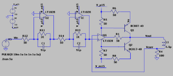
Hello , i have designed with a big help from this forum a driver.
at first glanse it amplified great the signal how ever when i probed R1 resistor as shown below on my lab scope with DC input , i saw oscilations.
Now when i did step responce of the circuilt as shown below i see the oscilations.
I also know from analog design course that i can try and see the AC responce.
LT1028 is -1 stable ,how does it influence the connection between the stages so i will not get oscilations.
What could cause instability in such configuration?
Thanks.

1704747020456.png


1704745962928.png

1704746912539.png


1704746711098.png
 
Output stage has additional loop gain created by transistors and phase lag due to inductor, so it's not necessarily stable.
 
Hi,

So the simulation worked (schematic)
The real circuit oscillates

but to find the issue you only showed us the (working) schematic.

It´s like: you have two cars, one is green the other red. The green one does not start ... so you give the red one to the garage for finding the problem.
--> What I want to say: If you encounter a problem with your real circuit, then show us your real circuit.

We don´t see the power supply, we don´t see that GND wiring. Both are "ideal" in a schematic .. this means "not realistic".

**********************
You also say the LT1028 is stable with -1
But U1 has a positive gain.

**********************

Klaus
 
Phase margin in simulated loop gain is rather small. But we can't be sure if real loop gain exactly matches simulation due to model inaccuracies, different load impedance, possible parasitic circuit effects like crosstalk to preamplifier. Additional compensation may be useful.

What's required driver bandwidth?

1704797933625.png
 

Attachments

  • lt1028_w_current_boost mod.zip
    1.4 KB · Views: 51
Was your scope probe set to x1 or x10 ?

Post picture of your prototype ......

What are you using for bypass caps on OpAmp supply pins ?

I get ~ 35 degrees of phase margin when doing bode sim, and following transient
response :

1704800679219.png


Regards, Dana.
 
The LT1028 was designed to maximize BW open loop at the expense of phase margin and has not been optimized for phase margin. There are external compensation pins not shown in my model or yours , yet they were ignored in your design.


I 'd like to remind everyone to design by "MUST HAVE" specs , then do whatever it takes to achieve your goals. The "NICE TO HAVE " specs are just bonuses.

I assumed you wanted to minimize overshoot to 2% and suppress resonances that cause sidebands in your YIG. But you need to specify values for EVERYTHING you anticipate as a fault.

Take # 21. Since you are not doing what I ask, you will have to observe or guess what changes I made to improve your results at 40% duty cycle for each stage normalized by gain changes.

Even this may not reflect your physical cable impedance and unknown lengths.

By your asking intelligent questions and searching for answers, you will learn, but a good design book is needed and better questions.
1704807967265.png


You can find the earlier chapters there.
 

Attachments

  • driver_even.mo.better.zip
    2.3 KB · Views: 51
Last edited:
Hello Mr. Stewart, yes you are absolutely right .There is a over-comp leg on the LT1028 which is not present in the simulation.
You even predicted the stability issue shown in the link below,so i am trying to follow my best with your advices.
So if i go back from where i started in the schematics shown below, could you please recommend me steps i should do to stop these oscillations?
Thanks.


1704810194794.png


1704810258684.png


1704810719413.png
 
No.

Start with full design specs for good performance and errors like overshoot, and component availability, lead time, project time / budget limit.

For example, I could better performance with a different IC, but you insisted no change for no good reason. For example is this for an undergrad thesis or a private company. Do you have time to re-spin the PCB or not. Is this for qty=1 or future volume=?
 
Last edited:
The LT1028 was designed to maximize BW open loop at the expense of phase margin and has not been optimized for phase margin.


From datasheet "The LT®1028(gain of –1 stable)/LT1128(gain of +1 stable)"

Then we have :

1704811632166.png


So phase margin definitely a cliff hanger, but then Cload curve they snuck in
some G rolloff in test circuit.

Then we have this (thanks ADI for a "guess what to do with this pin" approach) :


Regards, Dana.
 
Then we have :

View attachment 187663

So phase margin definitely a cliff hanger, but then Cload curve they snuck in
some G rolloff in test circuit.

Then we have this (thanks ADI for a "guess what to do with this pin" approach) :


Regards, Dana.
The non-inverting input is better if the source impedance is not 0 and will be better to reduce the negative feedback overshoot. Thus the phase margin is improved by increasing risetime (slightly) for any Rs source.

Clues
1704813096714.png
 
Last edited:
Hello , my specs are 20mA threw the could so my YIG will move 12MHZ from end to end.
My components are not burning because i lowered the DC supply so there is no problem.
the only spec is i put DC voltage in the input and i get a steady DC (with no oscillations on the output).
My voltage input is from 0 to 10mV pk-pk and it need to ne 20mA.

reading the data sheet they say i show connect the capacitor from this leg 5 to the output.

I can try in real life to input a step response to my circuit and see the overshoot on the output.( to see phase marging issue)
So by the phot below i need to connect a capacitor between opamp output to ground and see how it handles overshoot?( and its an alternative to use leg 5 OVERCOMP)
If its this a good idea, i will start by putting 90pF?
Thanks.


1704812881425.png
 
That is not an adequate design spec for your circuit. A design spec is a table of parameters, with tolerances {min:max or Nominal: +/-%} and test conditions (assumptions) listed for each like a datasheet. You get better at this with practice.

It should list all the critical requirements found in component datasheets then you choose the components that meet it and include tolerances of resistors and all passives required including source , load , cable impedance+ lengths, supply specs etc.

If you were designing an Op Amp, like the LT1080, I would expect a design spec to include the following. But your requirements are much relaxed so this Op Amp is "overkill" for both cost and yet under-compensated for step response. Ideally you want critical-damping. Do you know how that is defined? You must also define your environmental specs like a "benign" lab using 25'C or outdoors with full temperature range shown below or something in between.

1704813913938.png

1704813753575.png
 

Attachments

  • 1704813579948.png
    1704813579948.png
    97 KB · Views: 34
Last edited:
Generally speaking adding Cload aggravates phase margin because the Zout
of an OpAmp is inductive in nature, rises as gain is lost as frequency rises.

You can compute this by doing a LaPlace analysis of Zout for 1 and 2 pole OpAmps.

1704814416786.png


Regards, Dana.
 
If you do not have LTspice, install it and learn how to use it then open the Zip and open the .ASC file or extract it to your folder, Documents\LTspiceXVII\examples then open the *.asc schematic file and run it then add probe points. Use Labels, Measure current inside components or Voltages outside with pointer on schematic. Add gain equations to Edit plots to compare easily each stage. Modify current with R value changes. Simulations can be done in 5 minutes with practice. trial and error by PCB changes can take weeks when you do it the way you have.

1704815265157.png

--- Updated ---

I never had these tools in my career, so I just learned how to use it in the last couple months.
But you can use LTspice for WIn10 or XVII for Win 7 which I greatly prefer.

But experts will prefer MATLAB or use Python or even better free MICROCAP 12 which I have not mastered yet, or Simetrix which @dana uses or many many other tools. Your career will depend on you mastering some of these tools and more.
--- Updated ---

The design specs are Oscillating here. (silent c)
 
Last edited:
Your schematic had many jogs in its wiring (caused by Multisim?) and it had its parts very far apart making it huge.
I fixed it:
 

Attachments

  • cropped schematic.png
    cropped schematic.png
    42.4 KB · Views: 44
Your schematic had many jogs in its wiring (caused by Multisim?) and it had its parts very far apart making it huge.
I fixed it:
Thanks AG but I did it intentionally to show the logic of avoiding a large feedback loop for whatever reasons like avoiding parasitic coupling to the positive feedback Vin+ in the layout.

Then corrected the distortion from -ve feedback by using Vin+ with gain adjusted for 50 mA , which is now apparently 20 mA. from 50 and 100 mA before.,
 

Attachments

  • driver_even.mo.better.zip
    2.3 KB · Views: 48
Last edited:
Hello Mr. stewart ,your circuit looks quite different from the structure i have made.
When i ran the simulation i get this current threw a coil far from the expected rectangular shape.
and i use 7.5 Volts not 15 because my components were butning with 15V.

I need to think of a method on how to investigate stability in real life and see how exactly its getting better of worse.
Could you please recommend me how with lab equi[ment i can see if my stability get better or not?
Thanks.

1704915893730.png

1704915741018.png


1704915802617.png

--- Updated ---

UPDATE:


My circuit has a very simple goard i put DC voltage of 10mV and i get 20mA on the inductor.
pure DC signal.
My goal is to learn how to investigate stability issues of a circuit i have built
I can do LTSPICE sinulations to learn how to tune the circuit into stability.
There could be many issues, maybe i have noisy power supply .
Maybe i have bad decoupling circuit.i need to learn how to investigate in real life.

suppose i have oscilations on my scope instead of DC, how can i know the phase margin situation from it?
looking at the AC responce i cant see anywhere a point where i have 0dB and 180 phase(barkausen condition)

Thanks.

1704918993861.png
 
Last edited:
Hi,
When i ran the simulation i get this current threw a coil far from the expected rectangular shape.
the problem is that you ignore how an inductance works.

dI = V/L

it says: if you want a high rise rate in current (like the edge in a square wave) --> you need to apply a high voltage.

But for the advantage of low power dissipation you reduced the voltage. Now you miss the voltage to achieve a rectangular current waveform.

I can´t remember that you specified a rectangular waveform before. Maybe you did. If you did not: don´t complain!

Klaus
 

LaTeX Commands Quick-Menu:

Similar threads

Part and Inventory Search

Welcome to EDABoard.com

Sponsor

Back
Top