Continue to Site

Welcome to EDAboard.com

Welcome to our site! EDAboard.com is an international Electronics Discussion Forum focused on EDA software, circuits, schematics, books, theory, papers, asic, pld, 8051, DSP, Network, RF, Analog Design, PCB, Service Manuals... and a whole lot more! To participate you need to register. Registration is free. Click here to register now.

Manufacturability of padless vias

Status
Not open for further replies.

abaz

Member level 2
Joined
Apr 26, 2011
Messages
51
Helped
7
Reputation
14
Reaction score
7
Trophy points
1,288
Location
Berkeley, Australia
Activity points
1,609
Taking into account my clearance constraints and polygon pours for power supply nets on a BGA device, I find that I'm not getting much connection metal between the vias that are not power supply ones.

If I have full stack vias going through a multi layer board and decide to remove via pads on layers that the via is just passing through is this a problem for PCB manufacturers or can they all do it. I'm particularly interested if this is possible on the top and bottom layers, where I can make the pad diameter the same as the hole size, giving me more width in my polygon pours or traces going inbetween vias

Any thoughts or experience on this matter would be greatly appreciated

 

Most PCB manufacturers have a minimum hole-to-pad size, I believe this affects the ability to create plated-through-holes. I'm not quite sure what your issue is-there are standards for your BGA footprint-the chip manufacturers generally have suggested layouts . You say that you want to have no pad on layers where the via is just passing through. By definition, there won't be a pad there, just a copper clearance (for internal layers). However, if you have vias on outer layers with no connection, you might want to consider using blind or buried vias if you really have spacing constraints. That's more costly.

Bottom line is, you should probably consult the PCB house and find out what their capabilities, requirements are.
 
  • Like
Reactions: abaz

    abaz

    Points: 2
    Helpful Answer Positive Rating
Most PCB manufacturers have a minimum hole-to-pad size, I believe this affects the ability to create plated-through-holes. I'm not quite sure what your issue is-there are standards for your BGA footprint-the chip manufacturers generally have suggested layouts . You say that you want to have no pad on layers where the via is just passing through. By definition, there won't be a pad there, just a copper clearance (for internal layers). However, if you have vias on outer layers with no connection, you might want to consider using blind or buried vias if you really have spacing constraints. That's more costly.

Bottom line is, you should probably consult the PCB house and find out what their capabilities, requirements are.
Thanks for the reply.

Yes I will contact the board house but I just wanted to know if this was do-able with standard manufacturing techniques for future reference.

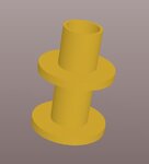
Here's a graphical representation of what I mean
The first pic shows the via with pads on all layers (for some reason its not showing pads on the plane layers?)
WithPad.jpg
The second with pads only on selected layers.
Padless.jpg
My presumption is that they drill and electroplate the holes. If the hole hapens to be where a pad is etched on that layer then it has a pad on that layer, otherwise it doesn't.
What I am unsure of is wether or not a pad is required on the outer layers to get the electroplating process to begin
 

Just got a reply back from the board house (PCB CART)

Thanks for your contact first,

You just want to do the "through" vias as per the Padless.jpg picture, right? if so, we can do them as per your file designed,

and it is a standard process with no addtional cost, many thanks, pls feel free let us to know if you had any further questions.

Best regards,
Zhao

> Hello
>
> I have attached 2 pictures to help explain my question
>
> If I have a multi-layer board and place a "through" via (NOT blind or burried) can I not have leave the pads off on selected Internal layers and more importantly, the outer layers
>
> If this is possible, is it a standard process with no additional cost or is it a special process that costs extra
>
> Thank you for your time

The two pics I attached are the ones in the above post

So, while not quite blind or burried, certainly more room on layers where we don't have to connect to... sweet!
 

The standard is to have no via pads on unconnected inner layers but always pads on top and bottom layer. At the outer layers, you'll need at least a minimal pad to compensate for drill tolerances. If the photo mask around a via isn't completely open, correct via metallization isn't guaranteed.
 

The standard is to have no via pads on unconnected inner layers but always pads on top and bottom layer. At the outer layers, you'll need at least a minimal pad to compensate for drill tolerances. If the photo mask around a via isn't completely open, correct via metallization isn't guaranteed.

Thank you for your input FvM, not knowing the process what you say now concerns me a little.
Are there any good sources of info on how PCB's are manufactured?
If there's a risk I'd like to understand it little before taking it.
I'll start searching now...
 

As I originally posted, I, too, believed that you needed pads on the outer layers, but your board house said it is 'standard'. I'm not an expert, but I would check another vendor. Just doesn't sound right to me.
 

I hate researching these things as it always raises more concerns.

I have managed to find out more about vias, or plated through holes but haven't been able to find out the process or more importantly the order in which they carry them out.

Given that they use electroplating to create the via walls there has to be an electrical connection to the hole so that electrolysis can begin.
The drilled hole is initially non-conductive so they "activate" the hole by chemically "seeding" it. A deposit of conductive liquid is placed in the holes by submerging the board in various chemicals.

Once this is done it undergoes electrolysis were the copper starts growing from pad out.

Given a normal plated through hole structure with a pad on bottom and top layers the copper grows from the 2 pads towards the centre of the hole. This is where a thing called the "aspect ratio" becomes important. It’s the ratio if the holes diameter to the thickness of the board. If the hole is too small and/or to long then the centre of the plated through hole becomes thinner.

Initial continuity tests will reveal the hole as conductive, but heat stress during soldering processes may cause the barrel to fracture. You can imagine the types of faults that may manifest as a result of this fracture. For example you may have continuity with the board off but powered up, heat generated on the board will cause expansion, open circuiting the hole.

What I don’t know, is the board already etched before electrolysis begins? On multilayer boards is it done after the board is laminated?

One scenario where I could see the padless outer layer PTH working would be if they drilled and etched the inner layers, only drilled the outer layers, laminated them all together then electroplating and then etching the outer layers.

I can’t understand how electroplating would work if the board was already etched. Given the small features in the artwork where 4/4 or 5/5mil track/spacing is present, wouldn’t electroplating create shorts?

If the process is similar to my assumed one, then I could see it working as the barrel is formed before etching the outer layers.

Any thoughts?

Edit: Seriously c r a c k is a sensored word. This is an electronics forum not a loosers/users forum!
 

You'l find detailed description of the production process on some PCB manufacturer homepages. On the other hand, even if you understand the basic process, you're not necessarily able to derive the constraints and design rules.

As a brief explanation about structuring outer layers.

The usual process starts with a thin copper layer on the outside (e.g. 18 µ for 35 µ finished thickness). The process sequence (without auxilary steps)

- drilling
- electroless copper deposite
- negative masking
- galvanic copper
- galvanic tin or nickel (working as etch resist)
- mask stripping
- etching
- surface finish

Some manufacturers are possibly using alternative processes that can give a different picture with different constraints.

A regular via/pad design rule wants to keep a closed annular ring in presence of drill tolerances and back- respectively under-etching. This leads to a minimal annular ring of 0.1 to 0.2 mm, depending on design class. A "padless" via would still need sufficient copper and etch resist metal plating to prevent damage of via metallization in etching step. So you can possibly save 50 or 100 µm from a regular designed via pad. IMHO it's a kind of dead end. The manufacturer would need to suspense his regular design rules, a via that is normally considered defective has to be accepted as intended and so on. Most manufacturers won't want to do this for understandable reasons.

If wiring space is really so rare, you would usually go for burried or blind vias or a combination of both.
 
  • Like
Reactions: abaz

    abaz

    Points: 2
    Helpful Answer Positive Rating
Thank you FvM

I was thinking along the same lines.

Stipulating a pad size the same as the finished drill size wouldn't be enough. You would have to take into account the finished wall size. Then there's dill placement tolorances, drill wable (Hole shadow?) etc, etc... which pretty much equates to what most board manufactures specify as the minimum anular ring.

I guess my conclusion is that this is something that should be avoided.

Thank you FvM and Barry for your input
 

Try and get the IPC-2222 specifications, they go into detail on land to hole ratios. Most PCB's are designed to class 1 2 or 3, 3 being the most stringent.

- - - Updated - - -

Slide 6 onwards explains hole to land ratios and why they are used.
http://dcchapters.ipc.org/assets/pnw/presentations/20060718_BGADesignGuidelines.pdf
 
  • Like
Reactions: abaz

    abaz

    Points: 2
    Helpful Answer Positive Rating
Thank you marce, its only through this recent search that I have come accross these design classes
 

Status
Not open for further replies.

Part and Inventory Search

Welcome to EDABoard.com

Sponsor

Back
Top