Continue to Site

Welcome to EDAboard.com

Welcome to our site! EDAboard.com is an international Electronics Discussion Forum focused on EDA software, circuits, schematics, books, theory, papers, asic, pld, 8051, DSP, Network, RF, Analog Design, PCB, Service Manuals... and a whole lot more! To participate you need to register. Registration is free. Click here to register now.

How to change the threshold of voltage difference between source and drain when the gate voltage is zero

Status
Not open for further replies.

henry kissinger

Member level 2
Joined
Nov 19, 2021
Messages
44
Helped
0
Reputation
0
Reaction score
0
Trophy points
6
Activity points
442
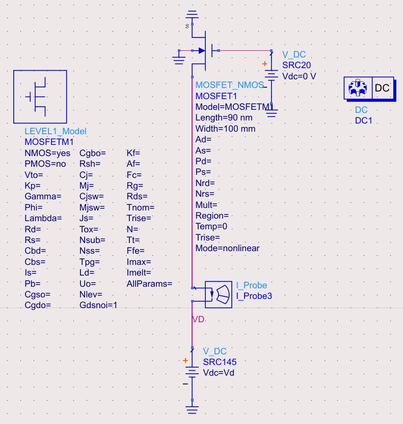
The NMOS configuration is as below.
the gate voltage is 0 V
the source voltage is fixed to 0 V, the drain voltage is swept from -2 V to 2V.
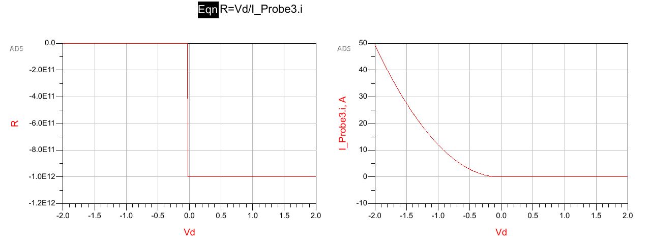
We can see that the threshold of voltage difference between source and drain is very little, at drain voltage around -0.01 V.
What parameter of this NMOS shown in the second graph (Level1_Model) I can change in order to have the threshold voltage difference much negative, say -10 V ?
nmos.JPG
Resistance.JPG
 

What "threshold voltage" are you talking about?
Normally that's the Vgs where the MOSFET just starts to conduct, and that does not vary significantly with a change in drain voltage.
 

Symmetrical FETs have no dedicated "drain" and "source". The function is switched according to the voltage difference between the channel terminals. In so far your interpretation of results misses the point.

In addition, do you realize that negative "Vd" puts bulk diode in forward bias. You see Vbs rather than Vgs threshold.
 

Status
Not open for further replies.

Part and Inventory Search

Welcome to EDABoard.com

Sponsor

Back
Top