Continue to Site

Welcome to EDAboard.com

Welcome to our site! EDAboard.com is an international Electronics Discussion Forum focused on EDA software, circuits, schematics, books, theory, papers, asic, pld, 8051, DSP, Network, RF, Analog Design, PCB, Service Manuals... and a whole lot more! To participate you need to register. Registration is free. Click here to register now.

[SOLVED] High power LDMOS matching issue at GSM band.

Status
Not open for further replies.

adnan012

Advanced Member level 1
Joined
Oct 6, 2006
Messages
468
Helped
2
Reputation
4
Reaction score
2
Trophy points
1,298
Activity points
4,923
hi,

I am designing a n amplifier for GSM BTS. I have selected MRFE6S9125N for my design. Previously i have successfully designed GSM amplifier by using PD20015-E fro ST.

I want to use MRFE6S9125N at 30 to 40 watt output with 28v dc.
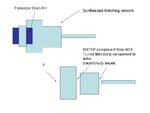
I am facing difficulties in extracting the optimum load impedance for specific output power and efficiency. I designed a prototype by using ADS MODEL of MRFE6S9125N. i Adjusted its gain at 15db from 925MHz to 960MHz by using VNA .

When i energized the amplifier by driver stage it burned at 10 watt
output power. (gate and drain both short to ground).

Is there any problem in matching network. What is the correct method of finding input and output impedance from datasheet and ads model?

Here is a document on Amplifier design. (from Very Good-Rf Power Amplifiers For Wireless Communications - Steve Cripps, Artech House,2006)

What is the significance of having load impedance high or low than optimum load impedance Ropt, as described in this chapter. i think my amplifier has been damaged by 2VDD swing.
 

Attachments

  • Power Amplifier Design 2.pdf
    250.2 KB · Views: 201

impedance can be found by simulating S11 or S22 over the frequency band
 
Thanks for reply.

Is it possible that improper output matching causes the total voltage swing greater than 2VDD or beyond device break down voltage.

- - - Updated - - -

What is the difference in load line analysis and Loadpull analysis? Which method correct.

- - - Updated - - -

What is the maximum IDD for MRFE6S9125N? It is not mentioned in datasheet.
 

Q) Is it possible that improper output matching causes the total voltage swing greater than 2VDD or beyond device break down voltage.

I don't think so!! swing depends upon your bias point.. it can't go beyond 2VDD other wise it will clipp!!!!

Q) What is the difference in load line analysis and Loadpull analysis? Which method correct.

Load pull analysis= what load at output can extract maximum efficiency or power out from transistor i.e. how much impedance should be there at output of transistor to extract max power!!
AC load line= tells max swing allowed
DC load line = tells where to select bias or operating point.
load line analysis= (have a look at attached doc)
load pull is more accurate.

Q) What is the maximum IDD for MRFE6S9125N? It is not mentioned in datasheet.

max VDD=28 V.
simulate S22 at your frequency band without matching network inserted (only transistor terminated with 50 ohm ), this will give impedance offered by drain at different frequencies,from this graph take max impedance ...... divide VDD= 32V with real part of that located impedance you wil have max current allowed....!!!
 

Attachments

  • L07 DC and AC Load Line.ppt
    399 KB · Views: 107
Last edited:
The given information is very few and that's why it's hard to say something for a solution.
But in ADS Load Pull Design Guide can be used to find Optimum Load Impedance for your Power Amplifier.
Nevertheless, don't trust too much nonlinear model of the transistor instead ask to manufacturer for real-world measured Load Pull data.
 

Blowing at only 10Watts sounds like there might be an Oscillation on the Voltage lines.
Also from the data sheet, setting the gain to 15dB seems like it might cause an issue. They are
stating 20-19dB is typical. If you look at the gain circles, by going from 19-ish dB to 15dB you will
need to change the I/P & O/P impedance of the PA.
Look at pg 9 & 11 of this file, to get an idea of what can happen by changing gain levels. Also keep in
mind that Pmax requires the PA to be non-linear and the PA's Impedance changes as the IC becomes
non-linear (Load-Pull). So the Data sheet has all these factors accounted for.

In general you should not deviate too much from the Data sheets guidance, or you will
have to work out all the bugs that comes with it.

Cheers
 

Attachments

  • ch11.ppt
    2.2 MB · Views: 140

Thanks for reply.

I am investigating the issue.

The attached picture contains an arbitrary output matching network. to solve discontinuity issues ADS MSTEP component is used. Do i need to use it at the transistor side too? The test board of MRF6S18060NR1 as shown in datasheet have a larger transmission line patch attached to the transistor. Is it necessary to pay attention at this discontinuity.

These pages are from cripps book. Page 26 and 27 says that total voltage swing can be greater than 2vdc.
 

Attachments

  • Slide1.JPG
    Slide1.JPG
    39.2 KB · Views: 133
  • Linear_Power_Amplifiers.pdf
    2.5 MB · Views: 183
Last edited:

By investigating further, i found that MRFE6S9125N starts oscillation occasionally at frequencies below 20MHz. ADS LSSP simulation also shows that it is not stable at many frequency ranges. It starts oscillation any time when the amplifier power is switched on. Biasing supply is switched on first.
I terminated the amplifier input side with 50 ohm resistor and connected the output to spectrum analyzer and applied power, i measured 2.8 ampere drain current and fundamental oscillation at 10 MHZ along with many harmonics. The oscillation imostly occurs when the amplifier is turned on after a short turned off time .
 

Stability can be checked through K factor tool of ADS... your amplifier should be stable i.e. K>1 over all of your operating band... if not i then a small resistor in the gate can make it stable.....!!!!
 

i have simulated it but did not use lower frequency due to convergence issues.
 

Status
Not open for further replies.

Part and Inventory Search

Welcome to EDABoard.com

Sponsor

Back
Top