narayani
Full Member level 2
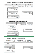
I have a load pull analysis values of Power Amplifier at Ka- Band 27 GHz for Maximum Power. Using Load Pull Analysis values of Zin (2.485- j11.369) and Zload (19.323+j59.271), I have designed the input and output matching circuits and tried to get values of S12 and S21 equals 0 and S11 and S22 below -15 dB using ADS tool. But I couldn't get values S21 and S12 equals 0 (zero) and S11 and S22 below -15 dB. Once I get these values, I want to get desired output power closer to 30.201 and PAE 53.467.
I have attched relavant screen shots. Somebody can help me to get desired values of Output Power and PAE.
I have attched relavant screen shots. Somebody can help me to get desired values of Output Power and PAE.
Attachments
-
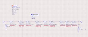 Input_Matching_Ckt.jpg325.9 KB · Views: 60
 -
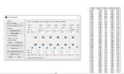 Tuned_Input_Matching_Values_.jpg304.3 KB · Views: 57
 -
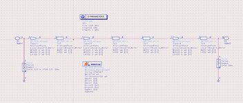 Output_Matching_Ckt.jpg255.2 KB · Views: 56
 -
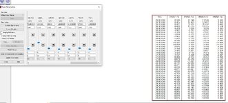 Tuned_Output_Matching_Values_.jpg375.8 KB · Views: 55
 -
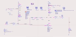 Main_Schematic.jpg153.5 KB · Views: 51
 -
 Main_Schematic_Output.jpg305 KB · Views: 53
 -
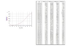
 Ka_Band_Load_Pull_Analysis_Results.png244.5 KB · Views: 54