chickenkill
Newbie level 3
Hi, friends~~
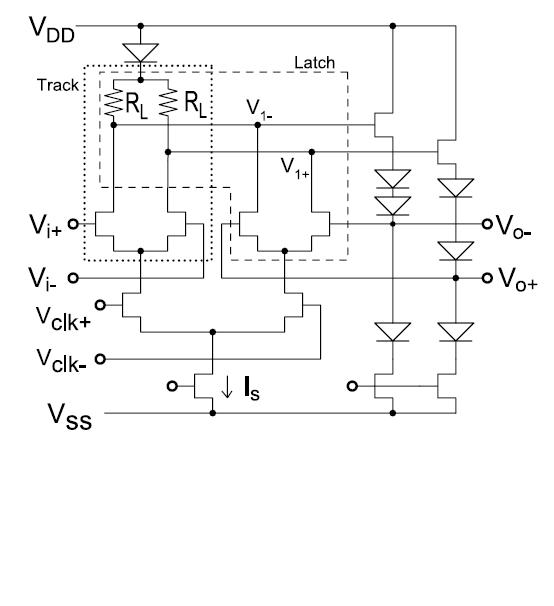
Recently I design a Gilber Cell comparator for Flash ADC demonstration by III-V process. I have refered some GaAs guys' design, and find they modified the prototype, and add a level-shift at the end for the feedback signal. (refer to pic)
I don't think such structure can enhance gain or speed. I guess Maybe the level-shift can low down the common-mode voltage, for protecting the Schottky Gate of second stage. Is it right? Because of the CMRR capability of diff pair, could us delete the level-shift for simpler design?
Another problem is about the layout routing. Typically, the diff pair should be loacted in symetry, but the design dismiss this rule for simpler layout. Is it acceptable?
**broken link removed**