Continue to Site

Welcome to EDAboard.com

Welcome to our site! EDAboard.com is an international Electronics Discussion Forum focused on EDA software, circuits, schematics, books, theory, papers, asic, pld, 8051, DSP, Network, RF, Analog Design, PCB, Service Manuals... and a whole lot more! To participate you need to register. Registration is free. Click here to register now.

Getting Error while optimizing power amplifier using ADS2022

narayani

Full Member level 2
Joined
Aug 15, 2014
Messages
120
Helped
0
Reputation
0
Reaction score
1
Trophy points
1,298
Activity points
2,262
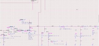
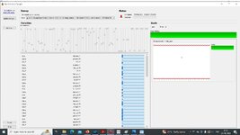
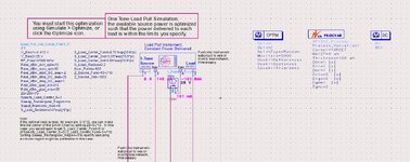
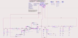
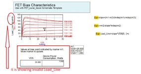
I am designing Power Amplifier at 27GHz. When I used template of one tone, constant power Delivered Load Pull and started executing, I am getting many errors. How to get out of this error? Error related screen shots are attached.
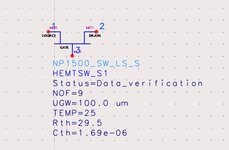
But when I connected template to only transistor. I didn't get any error at all. When I connected template to Power Amplifier Circuit. I am getting error.

Schematic_View.jpg
Error_Message.jpg
 

Attachments

  • Error_Word_File.txt
    77.2 KB · Views: 55
They are convergence errors. Check the circuit carefully and correct undesired connections such as shorted components, floating nodes, very high/low element values, loop branches.
You got many warnings and errors. There must be serious mistakes.
 
Wait what do you mean you connected the template to a PA circuit? Then it will behave as if (emphasis on as if) it were a 2 stage device since the load pull instrument already has the setting of a model PA connection without a transistor.
 
They are convergence errors. Check the circuit carefully and correct undesired connections such as shorted components, floating nodes, very high/low element values, loop branches.
You got many warnings and errors. There must be serious mistakes.
As you have given suggestion, I have modified the schematic values.
I have checked shorted components, floating nodes, very high/low element values, loop branches. Though I made all correction. Help me how to remove detected error,

Schematic.jpg
Simulation_Error.jpg
 

Attachments

  • Error_Text.txt
    26.8 KB · Views: 59
Why don't you do a ordinary HB simulation with a reasonable Input Power before doing optimization.
Check first the circuit works well and observe the AC voltage and currents to see any abnormalities are there or not. Optimization is the last step.
-DC Operating Point must be correct
-AC Current and Voltages shouldn't exhibit any undesired values
-50um X 4 NOF=200um periphery. Is that sufficient for high output power levels ?? Did you check the current density for wanted power level ?? For instance I used 1600um periphery for 26dBm Output Power for a wideband amplifier.
How about Load Line of your case ??
-Where are your Goals for your circuit ?? Where are your Measurement equations ??
 
Why don't you do a ordinary HB simulation with a reasonable Input Power before doing optimization.
Check first the circuit works well and observe the AC voltage and currents to see any abnormalities are there or not. Optimization is the last step.
Dear Sir, I have already completed ordinary HB simulation. It is working smoothly for AC Voltage and current and I wanted to do optimization of PA.
DC Operating Point must be correct
-AC Current and Voltages shouldn't exhibit any undesired values
Yes sir, I am getting correct DC Operating Point screen shots of the same same are attached below. Attachments are as follows.
DC operating point
DC operating points_1
DC operating points_2
DCIV_Characteristic
-50um X 4 NOF=200um periphery. Is that sufficient for high output power levels ?? Did you check the current density for wanted power level ?? For instance I used 1600um periphery for 26dBm Output Power for a wideband amplifier.
I have not understood what is 50 um x 4 NOF. Please help me to understand how to get desired value of 35 dBm power. Please help me to get 35 dBm output power. Please tell me how to take 1600 um periphery for 35 dBm.
Did you check the current density for wanted power level ?? For instance I used 1600um periphery for 26dBm Output Power for a wide band amplifier.
How about Load Line of your case ??
- I have checked the current density for desired power level and Load line is drawn.
Yes I have checked. Relevant attachments are as follows.
-Where are your Goals for your circuit ?? Where are your Measurement equations ??
- Yes, minimum power delivered is 10 dBm and maximum power is 25 dBm. Relevant documents are as follows
DC operating points_2.
I have attached the constant power delived screen shot.
--- Updated ---

Clarification, can we use the following attached HEMT nonlinear model for getting output power 30 dBm. Because this is only highest availble 900 um periphery. Screen shot of 900 um_HEMT is attached below.
 

Attachments

  • DC_Operating_Points_1.jpg
    DC_Operating_Points_1.jpg
    352.7 KB · Views: 63
  • Constant_Power_Deleivered_Load_Pull_Analysis.pdf
    300.9 KB · Views: 57
  • Error_Message.txt
    46.8 KB · Views: 80
  • Power_Sweep.gif
    Power_Sweep.gif
    19.1 KB · Views: 60
  • OPtimization_1.jpg
    OPtimization_1.jpg
    285 KB · Views: 59
  • OPtimization_1.jpg
    OPtimization_1.jpg
    285 KB · Views: 59
  • DC_Operating_Points_2.jpg
    DC_Operating_Points_2.jpg
    262.5 KB · Views: 54
  • DC_Operating_Points.jpg
    DC_Operating_Points.jpg
    126.4 KB · Views: 60
  • DCIV_Characterstics.jpg
    DCIV_Characterstics.jpg
    207.7 KB · Views: 57
  • 900um_HEMT.jpg
    900um_HEMT.jpg
    32.1 KB · Views: 61
Last edited:
OK, make your project archive (do not zip the whole project directory) including Process Design Kit then save this archive as RAR or ZIP. Post it here.
 
BigBoss Sir,
I have attached PA file including PDK. File name inside the folder is HB1_Tone_Loadpull constPdel. Please look into it and help me. I have sent a link, please click below link and download PA file
 
OK, I have downloaded the project file.

I'm sorry to say but you are on a absolutely wrong way. You're walking in the dark.
I will tell you few things to follow up.
-Load Pull technique is applied to ONLY the transistor itself, not whole circuit. When you find Optimal Impedance for any purpose (Max. Power OR max. gain OR max. Efficiency BUT NOT for ALL simultaneously) jump to other steps .
-Design an Output Impedance matching that exhibits exactly the Optimum Impedance which you have already found before. Use optimization here and observe the other specifications for the Class of the Amplifier ( harmonic terminations, levels, voltage and current waveforms etc.)
-Check the transistor with this OMN and observe the Operating Conditions AND the specification which you're interested in. Input Matching is NOT necessary for the time being on this step.
-You have optimized and got the values that you're interested in then work on Input Design Matching (Source Matching).
-Check overall Amplifier's Performance with IMN and OMN. Observe -again !!- Voltage and Current Waveforms. This point is important.
-Design your Layout and Simulate in ADS Momentum (or whatever you like). Check again overall performance of the PA and return back if it's necessary (probably you will) and again and again till you get the desired performance.

Otherwise you walk in the dark and loose your way.

Analog design is NOT easy as digital, you will iterate a circuit in many times and you'll live many non-event.

I cannot help you anymore because it's YOU who will correct your way and learn.

Note To whom it may concern : Search the Internet, you'll find millions of papers about everything. You can learn 10 times more that you have already learn in the school.
 

LaTeX Commands Quick-Menu:

Part and Inventory Search

Welcome to EDABoard.com

Sponsor

Back
Top