Continue to Site

Welcome to EDAboard.com

Welcome to our site! EDAboard.com is an international Electronics Discussion Forum focused on EDA software, circuits, schematics, books, theory, papers, asic, pld, 8051, DSP, Network, RF, Analog Design, PCB, Service Manuals... and a whole lot more! To participate you need to register. Registration is free. Click here to register now.

FET's blowing up occasionally in solenoid valve mains control circuit

Status
Not open for further replies.

userx2

Full Member level 3
Joined
Sep 19, 2008
Messages
165
Helped
2
Reputation
4
Reaction score
3
Trophy points
1,298
Activity points
2,990
Hello,
I must admit, I have always had problems with Fet's not lasting in many applications I have used them as well as seen used by others.
This ranges from welding machines, light dimmers, motor controllers etc.
I never found the real reasons why this happens.
One other designer told me once that he moved away changed his designs to use IGBTs instead since they do not seem to have this issue.

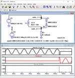
Now I have a circuit that a former colleague of mine designed into one of our products. This one controls a 240V mains operated solenoid valve.
Now, about a year or so down the line, failures have started to emerge where the Fet's are burned out and there is again no easy explanation.
I am now considering changing the circuit to use a triac instead. They do last but have more power dissipation and heat generation

Perhaps someone here has better experience and can share their thoughts what may be happening here?
The solenoid is 230V 6W

The circuit looks as attached. There are 2 Fets and 2 opto isolators to drive the gate voltage.
Either one or both Fets go faulty and will be cracked open or just black bits remaining.
I personally cannot find anything underrated or wrong with the circuit. The mains has MOVs on it as well at the input of the PCB.
Q2 and or Q6 seem to blow up. So far, it is 5 out of 200 delivered units and it happens after a month or longer. Hard to say what customers do with the unit.
The solenoid itself is usually found open circuit as well (yes open, not shorted).

Solenoid circuit 1.JPG
 
Last edited by a moderator:

Interestingly, in 90% failed cases we have so far, the same solenoid circuit has blown up.

Thats sounding off a big clue alarm. PCB layout ? Wiring introducing just
enough additional L to aggravate the problem ?

I notice there are no gate damping Rs, maybe this might be helpful :


Also the body diode is not exactly a fast device, in fact seems slow = bigger transient V's

1663106706346.png


If you can cycle the valve under program control, hang a DSO off the gate, set it
for triggering V that is out of spec for the part, single shot, and see if you get a
capture. Let it run for a few days.....maybe even randomly alternate opening and closing
the other valves as well. I have caught runts and other transients this way, very effective.

Regards, Dana.
 
Last edited:

Amongst heaps of other standards, these units have been tested and passed EC 61000-4-4 Electrical Fast Transient.
--- Updated ---

@danadakk
The gate damping resistor issue has come up before and we have tested this several times, with and without it. The result is always that it not required in this case. The switching waveforms are beautiful, no oscillations etc.

All the above being said clearly something is blowing up parts. Unless
you got defective/marginal parts from vendor, bad date code, package assembly
problem, there is something blowing parts.

Not a power sequencing problem in design.......

Have you delidded parts yet to see what actual failure mechanism is ? My methods of yore
probably no longer valid but we used to take them out into a parking lot, use a blowtorch,
and turn the plastic to ash. Then we could examine assembly and die issues. Actually worked
well and did not use the chems it takes to do it that way.

Good luck.


Regards, Dana.
 

I haven't looked that closely, but the first thing that jumps out at me is: what do R6 and C4 do? They're just dangling in the air, which makes me think you might have other errors in your schematic.
 

I now checked the DC resistance of this coil. It is 1k8!
The worst case peak current would be 240 * 1.41/1800 = 188mA. Even with tolerances, it might be as much 220mA max. I think we thus can rule out the problem of the zero cross on switching current.
Okay, it would seem clear we can rule out over-current as a possible cause of the failure.
what do R6 and C4 do?
Which schematic?
 

I haven't looked that closely, but the first thing that jumps out at me is: what do R6 and C4 do? They're just dangling in the air, which makes me think you might have other errors in your schematic.
Perhaps you should look more closely :) 😀
--- Updated ---

Have you delidded parts yet to see what actual failure mechanism is ? My methods of yore
probably no longer valid but we used to take them out into a parking lot, use a blowtorch,
and turn the plastic to ash. Then we could examine assembly and die issues. Actually worked
well and did not use the chems it takes to do it that way.
What would one see? I have in 35 years never tried to open a blown semiconductor. Interesting.
 

Myriad of failures, bond wires blown open to die, gate oxide failure (now potentially harder
to see because of geometries, eg. microscope needed), melted metal routes, die scrubin....
Keep in mind the geometries I looked at in the 10's of microns, now sub, so sem and
acoustic analysis more prevalent today for the finer stuff. I would guess under simple
magnification you can still see gross failures, and some not needing SEM analysis.

Most vendors have failure analysis docs showing pictures of failures. Check out their reliability
department links on their websites. I know IRF had a lot before they merged. If not on site
contact support and ask for rel handbook(s).


https://www.tti.com/content/dam/tti...peria-power-mosfet-design-engineers-guide.pdf CHAPTER 8


Regards, Dana.
 

It is getting worse, from an engineering point.
I have one here were the current sense resistor R35 is blown off the PCB. That is a 0.4W resistor and it would require 200mA to get to that Wattage. So for some reason, a higher than theoretically possible current has been flowing here. The FETs are still ok on this board.

I also just tested another one and the top FET has an interesting failure in that it has become shorted one way but diode the other way . Forward voltage is 400mV (the normal intrinsic diode voltage is around that) and reverse voltage 50mV.
I have never seen anything like that either.
 

Any chance you can get a hold of a DAQ and watch / datalog some nodes
over extended time to see if you can capture the conditions of failure.


Regards, Dana.
 

Hi,
I also just tested another one and the top FET has an interesting failure in that it has become shorted one way but diode the other way .
did you short G-S for this test? If not: do so.

Klaus
 

I replaced the FET yesterday and that PCB is working fine again. It was just that FET going funny. No other damage. I do not know if the associated solenoid coil went faulty on this unit.

@danadakk
I tried you incineration method yesterday, as I am rather curious. I have the inside of the FET exposed. The 2 wires burned away.
I cannot see anything like in your links though. BTW: this FET is a SOT223.
 

Post the best in focus pic you can get of it, hi res camera or best you have.

Regards, Dana.
 

Post the best in focus pic you can get of it, hi res camera or best you have.

Regards, Dana.
Tricky. Not successful with what we have in the lab. We have a microscope but no ability to take pictures. Unfortunately I left it in the office and will only be back there next Wednesday. I will take it home then and try my USB microscope for a picture.
 

Finally, I have now got some pictures of the blown FET up as suggested by danadakk.
Does this show anything useful?
The one corner may have broken off during "disassembly"
This is FET where it measured as a diode one way but short circtuit the other way

20220930082926.jpg
20220930083017.jpg
20220930083101.jpg
20220930083541.jpg


Regards
X
 

Not sure, is this a trench fet ? The hole sure looks like a gate oxide punch
thru from HV, and then shorts causing alum to melt on right side. Or could be
a hotspot that developed. A rel department could ID this quickly. This is a guess
on my part as my die knowledge is older than the great Egyptian Pharaohs.....


Regards, Dana.
 
Last edited:

This may not lead to a solution to the actual problem I am facing here as that still continues.

Nevertheless, it is interesting.

Do you mean that round thing on the left, in the middle of the silver pad could be a hole?

I am not sure how much it all got damaged during the heating process to burn off the housing.
I may have overheated it as it glowed very brightly. I used a Propane/oxygen silver solder torch we have in out factory.

I guess I will have to open a good one to compare.


X
--- Updated ---

Not sure, is this a trench fet ?

Regards, Dana.
The datasheet says:

"These high-voltage devices are Zener-protected N-channel Power MOSFETs developed using the SuperMESH™ technology by STMicroelectronics, an optimization of the well-established PowerMESH™. In addition to a significant reduction in on-resistance, these devices are designed to ensure a high level of dv/dt capability for the most demanding applications."

Here is a some info.

https://www.edn.com/stmicroelectronics-reveals-advanced-power-mosfet-family/#genecy-interstitial-ad
That is all I can find out.
I wonder what they mean by Zener protected.
 
Last edited:

Two things that bother me about the schematic:

One, the follower opto gate drive discharged by 100Kohms
G-S seems likely to be quite slow, might leave the FET
linear for a good while and have no real "OFF" authority
against any drain dV/dt. When dark you basically have an
open-gate FET. That is mysterious, at best. And we're not
dealing with "best".

Two, aside from the TVS I see no "catch diode" for solenoid
turnoff, to take that energy. If one FET remains energized
while the other is turning off, there could be an unrecognized
current return path out of the solenoid through something
brittle. Such as an unclamped MOSFET gate.

For failure analysis I would first want to know the mode.
Gate rupture tends to leave a G-S resistance. Burnout
would either make D-S leak, or open source bond wires.
Are either of these signatures present on failed devices?
It would be best to pull a set of I-V curves on the gate-
source (Vds=0) and drain-source (Vgs=0) bidirectionally,
maybe a 10uA current limit, so you can see what's done
gone and broke.

The missing silicon is peculiar, in the photos. You'd have
to find a way to put a lot of force on that. Or crack the die
electrothermally, which -could- happen. A question is, does
it, more than once?

That's a funny looking FET, it has a lot more "texture" than
old timey ones I used to see. Like 1/4 of it is different than
the remainder. Maybe it's a gate clamp patch or something.
Two things that bother me about the schematic:

One, the follower opto gate drive discharged by 100Kohms
G-S seems likely to be quite slow, might leave the FET
linear for a good while and have no real "OFF" authority
against any drain dV/dt. When dark you basically have an
open-gate FET. That is mysterious, at best. And we're not
dealing with "best".

Two, aside from the TVS I see no "catch diode" for solenoid
turnoff, to take that energy. If one FET remains energized
while the other is turning off, there could be an unrecognized
current return path out of the solenoid through something
brittle. Such as an unclamped MOSFET gate.
Thank you, all points noted.

Regarding point one, I have tested the decay of the gate voltage to quite fast. This FET has a low GS capacitance. I cannot categorically rule out what you wrote but so far, I have not observed any slow secay or floating behaviour. Even if it were all totlally floating, the most current could only ever be the same as when on.

About point two: The thing is that we operate at AC mains here. That rules out any use of a catch diode and it is the reason for the TVS.

The solenoids have a resistance of 1800 Ohm so any current they can supply is rather small and well below the FET rating.

Yet, failures do occur.
The whole thing is still a big mystery.

Also, only one FET is on at a time here, again because of AC.
 

Hi X
I calculated the inductance of the coil to be 27.4 H, which leads to a time constant of 15.3 ms with the wire resistance of 1k8 alone. This means that the voltage clamped by the TVS diode remains at around 420 V for several microseconds. Assuming a slow switch-off due to the 100k resistor and at maximum coil current, there will be a uA-current at an elevated RDSon-value, which results in a short time span with dissipated power at the FET in the watt range (see simplified simulation below). Depending on the frequency the coil is switched, the FET may overheat.
Regards
Mathis
 

Attachments

  • Clipboard02.jpg
    Clipboard02.jpg
    314.2 KB · Views: 132

Status
Not open for further replies.

Part and Inventory Search

Welcome to EDABoard.com

Sponsor

Back
Top