jamesportman
Newbie level 6
Hi,
I understand parts but getting confused, hopefully someone can help.
I have a CPU which needs the ROM to be sat starting at 0x2000, but the ROM is 0x8000 long, so it is misaligned, mounted from 0x2000 to 0x9FFF.
There is also a RAM chip which needs to sit at 0x0000 and is 0x400 size which is easy to sort.
If the ROM was sat at 0x0000, or 0x8000 say then it would be easy, the fact it is misaligned compared to its size is the issue.
I have seen loads of guides for straightforward setups but this seems more complicated.
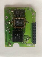
It is all working in an existing circuit with some unknown IC doing the magic, which is possibly a PLD or similar.
It is literally taking 0x2000 away from the address on the CPU/bus and passing it through to the ROM perfectly. 0x2000 is 0x0000 on the ROM address pins, 0x4000 is 0x2000, etc.
It is also managing the chip enables depending on the incoming address ranges, read vs write on the RAM,
also the bus is 8 bit data/16 bit address multiplexed, so it latches the address using ALE pin from CPU, there is also RD and WE pins on the CPU to help with this.
I figured I might manage with normal methods but on top of decoding, would end up needing to fix the address by subtracting 0x2000, which isn't straighforward, or is it?
Am I going to be better off just using a PLD or similar to achieve this?
Photo of existing board, the header pins go to CPU/mainboard.
Thanks,
James
I understand parts but getting confused, hopefully someone can help.
I have a CPU which needs the ROM to be sat starting at 0x2000, but the ROM is 0x8000 long, so it is misaligned, mounted from 0x2000 to 0x9FFF.
There is also a RAM chip which needs to sit at 0x0000 and is 0x400 size which is easy to sort.
If the ROM was sat at 0x0000, or 0x8000 say then it would be easy, the fact it is misaligned compared to its size is the issue.
I have seen loads of guides for straightforward setups but this seems more complicated.
It is all working in an existing circuit with some unknown IC doing the magic, which is possibly a PLD or similar.
It is literally taking 0x2000 away from the address on the CPU/bus and passing it through to the ROM perfectly. 0x2000 is 0x0000 on the ROM address pins, 0x4000 is 0x2000, etc.
It is also managing the chip enables depending on the incoming address ranges, read vs write on the RAM,
also the bus is 8 bit data/16 bit address multiplexed, so it latches the address using ALE pin from CPU, there is also RD and WE pins on the CPU to help with this.
I figured I might manage with normal methods but on top of decoding, would end up needing to fix the address by subtracting 0x2000, which isn't straighforward, or is it?
Am I going to be better off just using a PLD or similar to achieve this?
Photo of existing board, the header pins go to CPU/mainboard.
Thanks,
James