engr_joni_ee
Advanced Member level 3
Hi, my question is regarding this memory chip which is mt41k256m16tw-107-it. I guess this is 4 Giga bits memory or in other words it is 512 Mega bytes, right ?
 www.micron.com
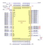
I just have seen in one schematic, see attachment that the addressing pins are from A0 to A14 and the data pins are 16 (D0 to D15). With 15 bit addressing how can we have 512 Mega bytes ?
What if only A0 to A12 are connected to the FPGA and T3 and T7 which are A13 and A14 are not connected.
How much memory in Mega bytes we still can have with address pins A0 to A12 ? I am not sure how the Banks need to include in calculations.
MT41K256M16TW-107 IT datasheet and parts catalog
Discover all you need to know about Micron's MT41K256M16TW-107 IT DDR3 with product specs, downloadable datasheets, and more.
www.micron.com
I just have seen in one schematic, see attachment that the addressing pins are from A0 to A14 and the data pins are 16 (D0 to D15). With 15 bit addressing how can we have 512 Mega bytes ?
What if only A0 to A12 are connected to the FPGA and T3 and T7 which are A13 and A14 are not connected.
How much memory in Mega bytes we still can have with address pins A0 to A12 ? I am not sure how the Banks need to include in calculations.
Attachments
Last edited: