Continue to Site

Welcome to EDAboard.com

Welcome to our site! EDAboard.com is an international Electronics Discussion Forum focused on EDA software, circuits, schematics, books, theory, papers, asic, pld, 8051, DSP, Network, RF, Analog Design, PCB, Service Manuals... and a whole lot more! To participate you need to register. Registration is free. Click here to register now.

[SOLVED] OPAMP simple circuit problem

Status
Not open for further replies.

seeker13

Junior Member level 1
Joined
May 18, 2013
Messages
17
Helped
0
Reputation
0
Reaction score
0
Trophy points
1,281
Activity points
1,534
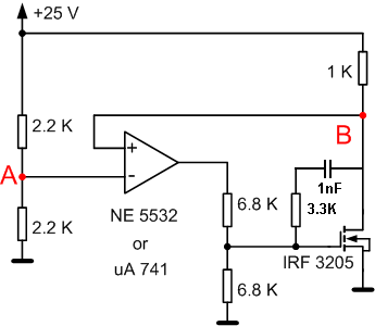
I thought I know the basic of OPAMPs and MOSFETs, so I tried designing a simple regulator, but the voltage measurement goes against all I know. I would be really grateful if someone would enlighten me about the behavior of this circuit.
In a nutshell:
---------------
I measure very large voltage difference between A and B (more than hundreds mV, up to 1V) - shouldn't it be very small (up to few mV)?

More detailed explanation:
--------------------------------
I implemented a negative feedback via non-inverting input of OPAMP, and the voltages on OPAMP inputs (points A and B) differ by more than 500 mV. AFAIK, both points A and B should be about 12.5V, and the difference shouldn't be more than a few mV (at worst few dozen mV - maximum input offset voltage). What I measure is 12.7V at point A, but 13.4V at B!?
I thought maybe it was faulty chip (uA 741), so I tested with another one, even tried with other type of OPAMPs (NE 5532 and LM 358) - the large difference between inputs was still there. One other strange thing: when I connected a few more MOSFETs in parallel with the one shown here, the difference of input voltages changed with every MOSFET I added?

One final remark: in attempt to debug the problem, I reduced the circuit to the one shown here (what I actually tried to do was a power supply), and the behavior I just described pertains to this simple circuit.
Is someone has an idea why the voltages at points A and B differ so much, I'd love to hear it. Thanks!

5984073900_1368836713.gif
 

Hi,seeker,there is some wire connection could be change.
For NE5532,negative feedback means the feedback should connect with inverting pin.Below are detailed description:
assume NE5532 non-inverting pin is Vp,inverting pin is Vn;
A point should connect to Vp
IRF3205 is NMOS,should be replaced by PMOS;
 

The feedback is the correct way round for using an NMOS. How are you measuring the voltages? My guess is the the circuit is oscillating.

Keith
 
Hi
Always voltage of A is 12.5v
and at first time nmos is off
so v+ is 25v
and because of that v+>v- output of op-amp become +vcc so nmos become on
and v+ connect to Ground
and because of that v+<v- output of op-amp become -vcc so nmos become off
and always it is the behavior of your circuit...so you make an osillator ...congratulation!:grin:

Best Regards
Green Tree
 

Yes, adding the gain of the PMOS common-source amplifier to the loop without any added compensation will cause oscillation. And it's not necessarily simple to compensate for that.
 
Hello seeker13,

* I think, the explanation of greentree is not correct. The feedback is a negative one (for dc and low frequencies) - thus, the given explanation (based on dc values) is not correct.
* However, as mentioned by crutschow, the additional gain caused by the common-source stage increases the loop gain and may cause RF oscillations, BUT at first you have to answer the following question:
WHAT KIND OF POWER SUPPLY (single or split)?
 
My guess is the the circuit is oscillating.
Yes, because the MOSFET adds a lot of voltage gain in the forward path. The pic below shows one way to stabilize the circuit. The voltage gain of the MOSFET stage is now limited to 0.5 above 50KHz. That should be fine for any unity-gain stable opamp.

 
Hello seeker13,

* I think, the explanation of greentree is not correct. The feedback is a negative one (for dc and low frequencies) - thus, the given explanation (based on dc values) is not correct.
* However, as mentioned by crutschow, the additional gain caused by the common-source stage increases the loop gain and may cause RF oscillations, BUT at first you have to answer the following question:
WHAT KIND OF POWER SUPPLY (single or split)?

Hi dear LvW

and thanks:wink:
but still isn't clear for me! where is negative feedback on this circuit?
what's your explanation if it be split?

Best Wishes

- - - Updated - - -
 

Hi dear LvW

and thanks:wink:
but still isn't clear for me! where is negative feedback on this circuit?
what's your explanation if it be split?

Negative feedback needs NOT necessarily to be connected to the inv. opamp input.
Instead, there must be one single sign reversal within the feedback loop - in this case: inverting operation of the common source stage.
That means: DC operating point is fixed and stable - however, as already outlined by keith, crutschow and goodfreyl, most probably there is instability for large frequencies (BODE plot check).
 
Last edited:
Wow, I'm really impressed by the speed and helpfulness of this board! Thank you all very much for useful responses - if I knew I'd get answers so fast, I'd ask here a lot sooner instead of spending days trying to troubleshoot the problem myself.

On to the problem - in short, yes it seems the oscillations are the problem. I implemented the solution proposed by godfreyl, and it works for LM 358. BUT, if I tweak the circuit a bit, the apparent oscillations reappear. For example, if NE 5532 is used or if 2-3 additional MOSFETs are connected in parallel.
If I understood the logic behind godfreyls modification correctly, the smaller values of R and the larger value of C in the RC circuit between G and D should provide more stability. Based on this, I reduced the R from 3.3K to 220R and increased C from 1nF to 100nF - this seem to solve the issue for the values used in the test circuit I presented here, but I'm not sure what will happen when the load is changed (in my example it is 1K, however, in actual circuit this will vary widely), or when reference voltage (point A) is changed.

*Question 1: If this is taken to extreme, would R=0 and C=1uF (for example) ensure definitive stability for any OPAMP/NMOS/load combination used?

Additionally, I don't quite understand the mechanism behind this oscillations. According to what I was taught about OPAMPs, the more open loop amplification an OPAMP has, the better, you will reduce it via negative feedback anyway. What you all seem to be saying is there is some limit when too much gain is harmful (causes oscillations), or am I getting it wrong?

I'd really like to intuitively understand the physical mechanism of this - how do oscillations arise? The best I can think of is that OPAMP don't react immediately to voltage changes of B. For example, if B voltage rises, the output voltage of OPAMP should also start to rise (therefore decreasing back B, and nullifying the change). This "tries" to happen, but it takes some time (due to various parasitic capacitances in OPAMP and NMOS?) for OPAMP output to affect the B, and during this time B keeps rising. When NMOS finally starts to react to OPAMP output, B starts to decrease, but now same thing happens in reverse - the B keeps decreasing even below what is initial value was. After this stops, the "loop" is repeated. The final result is that B oscillates around the value of A with some amplitude (which is larger, the larger these "delays" are, and the larger the overall gain is).

*Question 2: Is this what happens here?

P.S. @ LvW: it will be a single power supply.

- - - Updated - - -

Hi dear LvW

and thanks:wink:
but still isn't clear for me! where is negative feedback on this circuit?
what's your explanation if it be split?

Best Wishes

- - - Updated - - -

greentree,

the negative feedback on this circuit works as follows: assume voltage of B increases above A. This means that noninverting input of OPAMP becomes more positive than inverting input -> the output of OPAMP starts to rise -> the NMOS gate becomes more positive -> NMOS channel resistance drops -> the voltage of B starts to decrease. Neglecting the time issue (which seems to cause oscillations), this should stop when B voltage is almost equal to A voltage
The inverse is applied if you assume B decreases below A -> OPAMP output is decreased -> NMOS channel resisance increases ->B voltage increases.

So, the circuit tries to neutralize any "attempt" of B to change -> negative feedback.
 

Hi seeker13,

you have described the cause of possible oscillations in the time domain - and, in principle, you are right.
You spoke about parasitic time delays, which in the frequency domain are expressed as phase deviations.
And it is much simpler to describe the effect in the frequency domain - for example, as follows:

You want to provide negative feedback, but you can do this for lower frequencies only because the opamp has phase deviations for rising frequencies.
Clearly spoken - 100% negatuive feedback is achieved for w=0 only (dc operating point).
The mentioned phase deviations cause the negative feedback to turn into positive feedback for very high frequencies.
This is not a problem if the loop gain magnitude for these frequencies is already below unity (0 dB).
However, in your case the additional gain stage increases the loop gain - and as the result its magnitude is still above 0 dB for the critical frequency limit.
Thus, there is one frequency with loop phase 360 deg (identical to 0 deg) and loop gain>0 dB. This fulfills the classical condition for oscillation.

If the selected single-supply operation - in conjunction with the mosfet stage - works, depends on the dc gain of this stage.

LvW
 
Circuit is unstable. It oscillate at 240kHz. Adding RC as godfreyl proposed makes it stable.
If your multimeter readings differ you may suspect oscillations of a circuit. Next time use oscilloscope if you can.
 

Yes, because the MOSFET adds a lot of voltage gain in the forward path. The pic below shows one way to stabilize the circuit. The voltage gain of the MOSFET stage is now limited to 0.5 above 50KHz. That should be fine for any unity-gain stable opamp.


Could you please explain how you arrived at this numbers (Av=0.5 at 50KHz)?

- - - Updated - - -

Hi seeker13,

you have described the cause of possible oscillations in the time domain - and, in principle, you are right.
You spoke about parasitic time delays, which in the frequency domain are expressed as phase deviations.
And it is much simpler to describe the effect in the frequency domain - for example, as follows:

You want to provide negative feedback, but you can do this for lower frequencies only because the opamp has phase deviations for rising frequencies.
Clearly spoken - 100% negatuive feedback is achieved for w=0 only (dc operating point).
The mentioned phase deviations cause the negative feedback to turn into positive feedback for very high frequencies.
This is not a problem if the loop gain magnitude for these frequencies is already below unity (0 dB).
However, in your case the additional gain stage increases the loop gain - and as the result its magnitude is still above 0 dB for the critical frequency limit.
Thus, there is one frequency with loop phase 360 deg (identical to 0 deg) and loop gain>0 dB. This fulfills the classical condition for oscillation.

If the selected single-supply operation - in conjunction with the mosfet stage - works, depends on the dc gain of this stage.

LvW

Thank you for additional explanation - so the key is to keep the amplification of additional stage at these frequencies below 1, right?
 

.....................................

*Question 1: If this is taken to extreme, would R=0 and C=1uF (for example) ensure definitive stability for any OPAMP/NMOS/load combination used?

..................................
No necessarily. At high frequencies the feedback can go through C directly to the plus (+) input of the op amp and cause oscillations from that path. Thus you need a series resistor to limit the high frequency feedback.

If you simulate the circuit with Spice, such as the free LTspice simulator from Linear Technology that many on these forums use, you can see the effect of changing the resistor and capacitor values. You can simulate both the small signal AC response to see the frequency-domain peaking and phase-shifts that causes oscillations and ringing, and also simulate in the Transient mode to see the time-domain response.
 
At closed loop phase at output must not exceed -150° at unity gain and this is criterion for stability in practice.
 

"Could you please explain how you arrived at this numbers (Av=0.5 at 50KHz)?"

The R-C time constant of 3.3k and 1nF yields a 50kHz corner frequency. If you have a series RC, the impedance Z below 50kHz is falling with frequency (i.e., capacitive) and above 50kHz it's flat at 3.3kΩ (i.e., resistive). The gain of a common-source amplifier with feedback is roughly equal to the feedback impedance Z divided by the impedance of what's driving it (here, 6.8kΩ); in other words, the MOSFET acts like an inverting op-amp with its gate acting as the "virtual ground" (although this virtual ground has a DC offset of Vgs). Therefore, above 50kHz the gain is 3.3kΩ/6.8kΩ, at low frequencies it has a large gain (that rises as frequency decreases) — below 50kHz it behaves like an op-amp integrator. The feedback devices cause the MOSFET to have a tight local feedback loop which is inherently stable, and which helps to stabilize the global loop too by reducing the gain.

An easy way to think of stability is that if you look at the loop gain (the gain experienced by a signal traversing the feedback loop once), if the gain is falling with a single-pole rolloff when you get to the unity gain frequency (often around 1MHz for popular op-amps) then it's stable. If the gain is falling with two poles or more, then it's unstable. The op-amp has already been engineered just to be stable with the gain it has with an internal single pole; if you increase the loop gain further, you'll push it to be unstable (because it has a bunch of poles at higher frequencies above 1MHz). And that's why the additional gain of the MOSFET drove it unstable.

As you've experienced first-hand, you can decrease the loop gain to make it stable again, but you have to stop decreasing it by the time the loop hits unity gain. This returns you to a single-pole rolloff again. That's why the 3.3kΩ resistor is there. If it wasn't there, then you'd have a 1-pole rolloff from the op-amp and a 1-pole rolloff from the MOSFET acting as an integrator—and the two poles would conspire to make it unstable (even if your new crossover frequency is much lower, like 200kHz; the two poles still drive it crazy). The resistor ensures the MOSFET behaves as a flat 0.5-gain amplifier rather than an integrator at the loop's unity-gain frequency. The choice to give it a gain of 0.5 was a conservative approach to doubly ensure stability (yielding 6dB additional gain margin); the decision to make the corner frequency 50kHz was also to give margin; 50kHz is one full decade below the op-amp's new crossover frequency of 500kHz (it was 1MHz, but introducing a gain-of-0.5 element brought it down to 500kHz), so you can be confident that the MOSFET isn't behaving as an integrator anymore.
 
Last edited:
Wow, thanks for the detailed response ZekeR. I'm afraid a good deal of what you tried to convey is a bit outside my knowledge on the subject (things like poles and pole rolloff), but I think I managed to get at least some basic points, so thank you again. I'll try to recap in some simple approximate math what you just described ("input" are the values of R and C, "driving" impedance Zdrive, and unity gain freq of OPAMP fug), please do correct me if I'm wrong:
1. fc=1/(2*PI*R*C) (Corner frequency)
2. Av = R/Zdrive (Gain of the NMOS for f>fc)
3. fug_total=fug*Av (Overall unity gain; OPAMP and NMOS)

And, if I understood correctly, as long as R and C are chosen so that:
4. Av<1 and fc < fug_total,
no instability will occur?

But, if this is true, why does the proposed solution works very well with LM358 (with unity gain of fug=1MHz) and not quite as good (using the same 3.3K/1nF RC combination) for NE5532 (unity gain of fug=10MHz, which should be even better, according to 4.) ?
Looking at the datasheets, maybe it has something to do with "internal freq. compensation for unity gain" of LM358, not specified in NE5532 datasheet (so presumably lacking for NE5532)?
 
Last edited:

5532 or 5534?

  • NE5532 is a dual opamp, internally compensated to be unity-gain stable.
  • NE5534 is a single uncompensated opamp, needs an external capacitor for unity-gain stability.

- - - Updated - - -

But, if this is true, why does the proposed solution works very well with LM358 (with unity gain of fug=1MHz) and not quite as good (using the same 3.3K/1nF RC combination) for NE5532 (unity gain of fug=10MHz, which should be even better, according to 4.) ?
Not too surprising. With the faster opamp you need to avoid having any additional poles up to say 5MHz, instead of 500KHz. i.e. You need to add a point 5 to your stability criteria:
5) no added poles below fug_total

OK, that's not a strict requirement, but they will cause problems that get worse the further below fug_total they are: slight ringing => bad ringing => outright oscillation.

The explanation Zeker gave, and you paraphrased, is a little oversimplified.
Most importantly, the MOSFETs gate-drain capacitance is in parallel to the 3K3 resistor and 1nF capacitor, so that will cause the gain to roll off again at some high frequency (i.e. add another, unwanted pole).

... and I just looked at the IRF3205 datasheet. The gate-drain capacitance with 12V across the MOSFET is nearly 500pF. Yikes! I didn't expect it to be anywhere near that high. No wonder you're having problems. Of course, with multiple parallel MOSFETs, there's more capacitance so the problems get worse.

Hmm, this calls for a bit of a rethink on the stabilization.

- - - Updated - - -

OK, with an NE5532, changing the 3K3 and 1nF to 330Ω and 10nF should work. That drops the gain of the MOSFET stage to 0.05 above 50 KHz, and sets fug to about 500KHz. The added pole due to Cgd is about 1MHz with one MOSFET, or 500KHz with two in parallel, which should be OK - it still leaves a phase margin of about 45 degrees.

P.S. That's the first time I've seen the term "fug".:-D I'm used to "ULGF" - unity loop gain frequency.
 
Last edited:
Phew, thanks - all this pole talk is really quite vague to me, so I'm sorry for funny terminology (and questions). For the consistency reasons I'll keep up with the fug variable, if you don't mind.

According to your example (0.5MHz --> 5MHz), shouldn't the added criteria be:
5) no added poles below fug_total*10

Which brings me to the main point I'm missing: How to find out where those added poles are? For example, how did you calculated the added pole due to Cgd?

Oh, and BTW - as I said, it works very well even for 3 MOSFETs but with the values of 220R and 100nF (I came to this empirically, but would like some approximate formula to have some generic solution for this topology), and I was testing on NE5532.
 

Status
Not open for further replies.

Similar threads

Part and Inventory Search

Welcome to EDABoard.com

Sponsor

Back
Top