Continue to Site

Welcome to EDAboard.com

Welcome to our site! EDAboard.com is an international Electronics Discussion Forum focused on EDA software, circuits, schematics, books, theory, papers, asic, pld, 8051, DSP, Network, RF, Analog Design, PCB, Service Manuals... and a whole lot more! To participate you need to register. Registration is free. Click here to register now.

Will my transistor blow up in this circuit?

Status
Not open for further replies.

pha0001m

Junior Member level 1
Joined
Jan 10, 2015
Messages
16
Helped
1
Reputation
2
Reaction score
1
Trophy points
3
Activity points
138
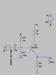
I am using the 2N5550 to build a simple buffer amplifier. This transistor has a Vce rating of 150V. I have constructed a circuit as attached bellow. This circuit will run on a 400V DC power supply.

I have tried to DC biased the transistor so that in the steady-state operating condition Vce is less than 40V. Thus, it should not blow up. However, what happen when the circuit is initially turn on? As I fear that the NPN will see the full 400V across at turn on. What do you guys think? Will this circuit work in practice?

Note: I do not want to cascode the transistor, nor do I want to use a NPN with a higher Vce rating.

Q1 baising.png
 

Attachments

  • Q1 baising.png
    Q1 baising.png
    6.4 KB · Views: 58

I would not trust it. The problem isn't due to the transistor, it's the coupling capacitor to the load. At the instant you switch on, and assuming you do not already have a voltage across the load, the emitter pin will be at a lower voltage until C3 charges up. Try simulating with the same resistor values but the emitter grounded and with a range of values for R11 to see what happens to the voltages.

I suspect you may also have problems with holding Vce at 40V as that simple bias arrangement will make it prone to variations in transistor gain and exact resistor values. When dealing with circuits where there is a potential for voltages to go beyond component specification, it is always better to design defensively.

Brian.
 

As you have sketched the circuit in LTSpice, did you already check the power-on transient behaviour in a simulation? It would be apprpriate to do so before asking general questions.

A possible problem that isn't yet addressed in your question is possible Vbe reverse breakdown during power-off, depending on the supply timing.

A simple solution towards fail-safe design could be to place a zener diode across CE which handles both overvoltage and reverse bias.
 

I would not trust it. The problem isn't due to the transistor, it's the coupling capacitor to the load. At the instant you switch on, and assuming you do not already have a voltage across the load, the emitter pin will be at a lower voltage until C3 charges up. Try simulating with the same resistor values but the emitter grounded and with a range of values for R11 to see what happens to the voltages.

Brian.

Yes, that is exactly what I am worry about, it will take some time for the emitter voltage to raise. I think FvM just gave me a solution by placing a zener diode in parallel with the collector and emitter.

So if I pick a zener voltage that is greater than the steady-state voltage Vce of 40V, let say if I were to pick a 100V zener, then I think it would safe to say that during turn on transient, the zener would lock Vce <100V, and during steady-state operation, the zener would turn off. Thus the transistor is protected at all time.

- - - Updated - - -

As you have sketched the circuit in LTSpice, did you already check the power-on transient behaviour in a simulation? It would be apprpriate to do so before asking general questions.

A possible problem that isn't yet addressed in your question is possible Vbe reverse breakdown during power-off, depending on the supply timing.

A simple solution towards fail-safe design could be to place a zener diode across CE which handles both overvoltage and reverse bias.

I had simulated it for transient behavior in LTspice, and there is no problem. It is properly because the supply circuit is a full-bridge rectifier design, thus the voltage ram up slowly due to the big RC time constant.

The zener diode is an great idea. Thank you! I don't why I did not think of that. I will give it a try.
 

While the input capacitor charges, at first it shorts the base to 0V then the 140V maximum rating of the transistor will be destroyed by the 400V supply.
Why does your 400V ramp up slowly? My full wave bridge rectifier power supplies ramp up almost instantly.
 

While the input capacitor charges, at first it shorts the base to 0V then the 140V maximum rating of the transistor will be destroyed by the 400V supply.
No, the voltage will be dropped at the 7k resistor in this state.
 

No, the voltage will be dropped at the 7k resistor in this state.
When the discharged input capacitor grounds the base of the transistor then the transistor does not conduct, there is no current in the 7k collector resistor thus no voltage drop and the entire 400V will be across the collector and emitter of the transistor unless it has avalanche breakdown.
 

While the input capacitor charges, at first it shorts the base to 0V then the 140V maximum rating of the transistor will be destroyed by the 400V supply.
Why does your 400V ramp up slowly? My full wave bridge rectifier power supplies ramp up almost instantly.

The rectifier circuit has a NTC thermistor connected at its input, and a 400uF smoothing capacitor in parallel with the output. The NTC thermistors create a big time constant during turn on. Thus the voltage ramp up slowly. It'll take about 1 second to reach 400V. The idea is to limit inrush current at switch on.

My opinion is this, at first the base is short to 0V, but the supply is also ramming up from 0V to 400V over a 1 second period. By the time the supply ram upto 140V, the emitter and the base voltage of the transistor have already risen. Hence, it won't see the full 140V.
 

Putting a proper zener diode ( for instance 150V ) juts after R4 will limit the VCE voltage because zener diodes are faster than transistors.
 

When the discharged input capacitor grounds the base of the transistor then the transistor does not conduct.
Yes, true. I was only thinking about output capacitor. Actual occurence depends however on the supply rise time, apparently it's not that fast.

Anyhow the discussion about possible breakdown has been superseded by the Z-diode solution.
 

Status
Not open for further replies.

Similar threads

Part and Inventory Search

Welcome to EDABoard.com

Sponsor

Back
Top