Continue to Site
Follow along with the video below to see how to install our site as a web app on your home screen.
Note: This feature may not be available in some browsers.
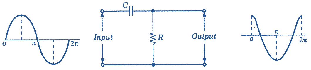
I recommend to differentiate betweenWe have basickly a difertiator
According datasheet, V_Z (3.6V) is measured @ I_Z of 60mA.Odd the Zener is supposed to be 3.6V but actual seems to be 3.2, model issues .
it is "r = 15 Ohms", not "R = 15 Ohms"Model is screwy because 15 ohms at 60 mA is .9v,