crazyboy
Newbie level 6
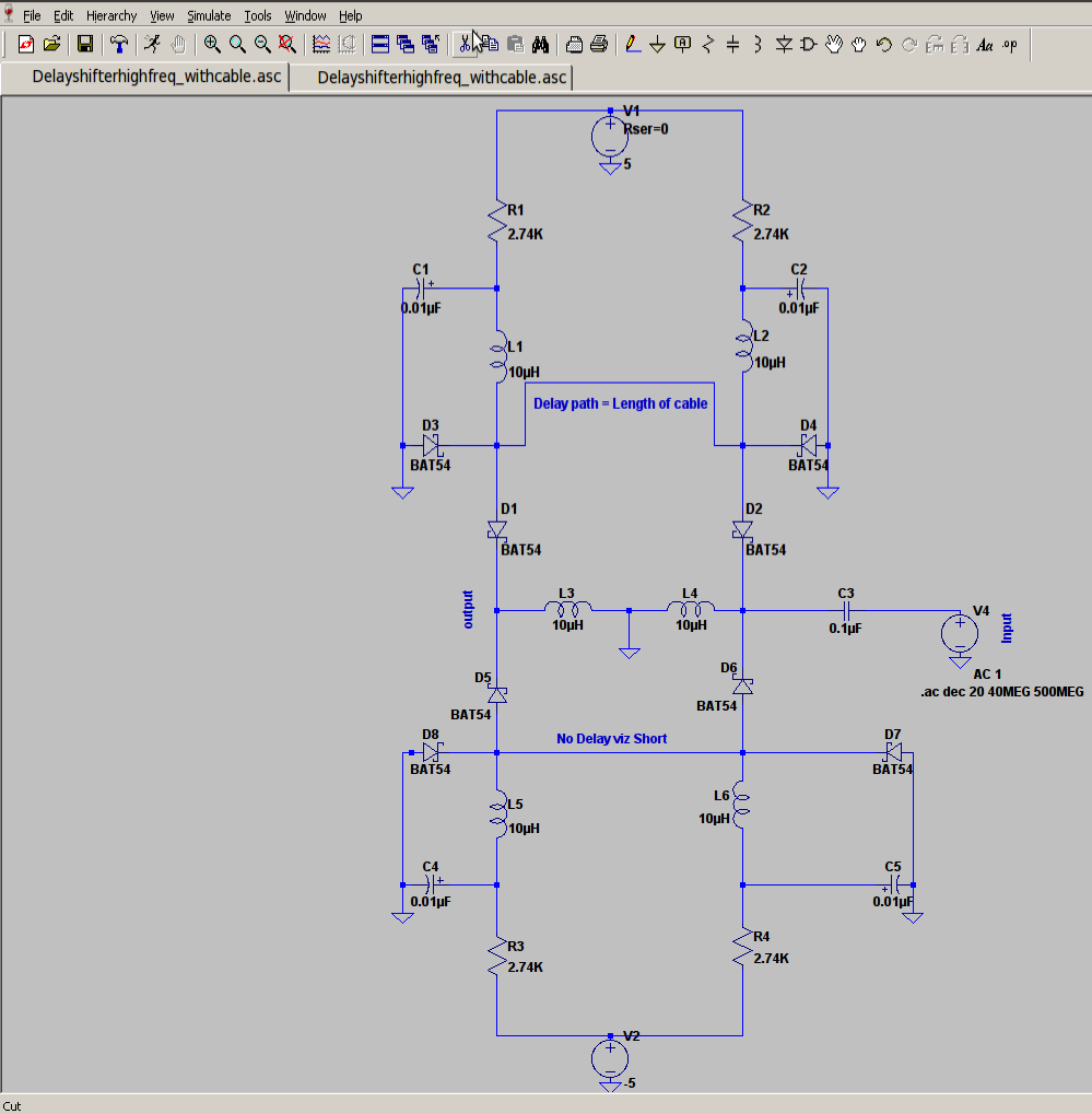
Hi friends can any one suggest a schematic of a wide band (30-500MHz) analog time delay circuit? I need a maximum time delay of 5ns with steps of few pico seconds. I will be very much thankful:-D.
Follow along with the video below to see how to install our site as a web app on your home screen.
Note: This feature may not be available in some browsers.
Hi friends can any one suggest a schematic of a wide band (30-500MHz) analog time delay circuit? I need a maximum time delay of 5ns with steps of few pico seconds. I will be very much thankful:-D.
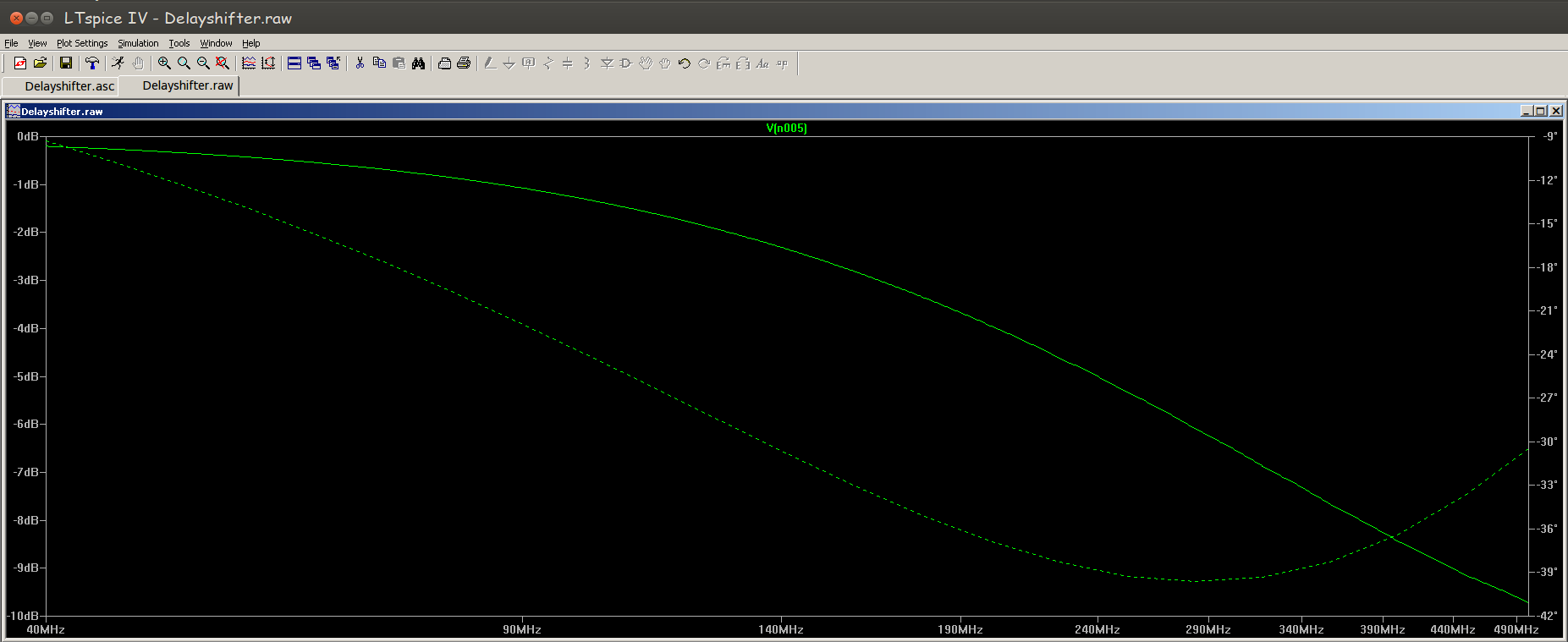
") . If this attenuation is not related to impedance matching, how can I achieve impedance matching for rest of band? (200-500MHz). As you told that the diode resistance and capacitance results in frequency dependent attenuation, can you suggest me a suitable diode for this requirement? The same is true for impedance matching as well? Because the LMR100 is perfect as it is impedance is well matched within the band. Please provide me a solution for matching the impedance throughout the band. I'm not bothering about the attenuation.
. If this attenuation is not related to impedance matching, how can I achieve impedance matching for rest of band? (200-500MHz). As you told that the diode resistance and capacitance results in frequency dependent attenuation, can you suggest me a suitable diode for this requirement? The same is true for impedance matching as well? Because the LMR100 is perfect as it is impedance is well matched within the band. Please provide me a solution for matching the impedance throughout the band. I'm not bothering about the attenuation.Hi I don't know how to do VSWR simulation in LTSPice. I Googled it and found nothing helpful. If you know how to do it can know explain briefly? Thanks in advance...
Hi I don't know how to do VSWR simulation in LTSPice. I Googled it and found nothing helpful. If you know how to do it can know explain briefly? Thanks in advance...
... Thanks a lot... cheers...