Continue to Site

Welcome to EDAboard.com

Welcome to our site! EDAboard.com is an international Electronics Discussion Forum focused on EDA software, circuits, schematics, books, theory, papers, asic, pld, 8051, DSP, Network, RF, Analog Design, PCB, Service Manuals... and a whole lot more! To participate you need to register. Registration is free. Click here to register now.

problem simulation delay line

yefj

Advanced Member level 4
Joined
Sep 12, 2019
Messages
1,195
Helped
1
Reputation
2
Reaction score
3
Trophy points
38
Activity points
7,217
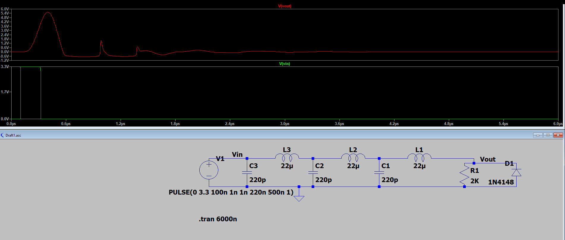
Hello , i was given a schematics which is supposed to be pulse delay .
my pulse is 3.3V and 220nS wide, but instead of a pulse on the outside i get a huge overshoot .
I know that LC system is a differencial equation which can lead to overshoot but its supposed to be a pulse delay.
Where did i go wrong?
LTspice file is attached.
Thanks.
1711374676646.png
 

Attachments

  • pulse_delay.rar
    715 bytes · Views: 40
Hello,how do i improve the delay line simulation,given that my pulse is coming from 33220A signal generator ?
Thanks.
 
what are your expectations? i.e. "specs"

(?). delay line filter critically damped with maximum BW and no diode reflections?

Define output Rise time, delay times , overshoot %, tolerance or stability, cost (?)
--- Updated ---

Easy to improve . Hard to know what you expect.

I might imagine this. Undershoot < 200 mV

E.g. using 50 ohm output and D.L. output into an XOR gate delay = 1 pulse width of 200 ns @ 1.667V ?? tuned < 10%.

1711380469049.png

--- Updated ---

or this ??

1711382254737.png

--- Updated ---

The leading and trail edge delays must also be spec'd which depends on BW, Q, group delay distortion, diode ESR*C (V)
 
Last edited:
Several LC stages are required to create a distinctive time delay. Each stage adds a little bit of delay.

Totaling 300 µSec with these values. The animated simulation (via clickable link to Falstad's) reveals numerous resonating loops persisting for many cycles. Damping effect may be achieved by experimenting with values.

tinyurl.com/263h48nb

delay pulse via several LC stages (8 series L)(8 caps to gnd).png
 
Characteristic impedance of LC resonator is sqrt(L/C). We see without detailed calculation that 1m/1u LC line is badly terminated with 470R.
 
Wave Ripple observations

  1. Neither the source nor load impedance dampen the 34% overshoot in the pulse response to the group time delay.
  2. The wave output shape is controlled by the Bode Plot and limited BW of this LC Ladder Low Pass Filter and the amount of energy in the passband from a narrow pulse.
  3. Mismatched source impedance does affect the amplitude after the source resistor. Although the ladder filter is lossless, and minimum group delay it is high ripple
  4. and the reflections of this pulse response from any mismatch of Zo=31.62 =sqrt(L/C)
  5. The series diode is equally mismatched and far less effective than the R-D shunt diode attenuators for overshoot.
  6. A Bessel filter would result in no overshoot with a known group delay.
So far all is silent from the O.P.

1711470288725.png
 
Last edited:
Hello Tony , so my 33220A is 50 Ohm in series with the idial voltage source ?

What is the theory behind doing this pulse delay?
I see that if I put a square pulse threw LC then it will be ruined . What is the logic of keeping the shape and controlling the delay?
I need a 300ns delay .
Thanks .
 
Last edited:
Examine the incoming Ampere waveform to get an idea what the emerging waveform looks like on your output resistor.

Even though you apply an initial square-ish Voltage waveform, the Ampere waveform is not identical. It's rounded. That initial Ampere waveform is similarly duplicated down the line from one LC stage to the next.

The first LC combination plays a key role in shaping the Ampere waveform. Smaller L causes quicker current ramp-up. Brief pulse causes less overshoot.

LC ratios do not have to be identical throughout. Even the simple Butterworth design uses different LC values in successive stages. A Bessel formula (mentioned in Tony's post #7) has LC values which are calculated to create a square-ish Ampere waveform.
Falstad's simulator menu has ready-made circuits which clarify these differences in filter types.
 
You only specified delay and load but you must also specify BW which determines N poles.

τg(ω)=−dθ(ω)/dω = group delay
What BW do you want? or risetime?

The Bessel filter has better shaping factor, flatter phase delay, and flatter group delay than a Gaussian of the same order, although the Gaussian has lower time delay and zero overshoot. The Chebyshev filter is best for rejecting side lobes with steep skirts.
 
Last edited:
Hello Tony, what is the role of the diode in the circuit shown below?
Thanks.

View attachment 189656
Your schematic has overshoot and if the signal goes into a CMOS ADC it may exceed max specs with ringing. Current limiting before diode is necessary if the limits are +\- 0.2 outside supply rails. A better filter helps too which may serve many requirements for stop band attn., risetime and overshoot.
 
Diode opens if certain value of the anode is higher above the cathode .I want it to limit at 3.3V.so I should reverse the diode because it will open up with the reverse rating of 15V :)

The more important thing to me is the basic theory.
I know how to design chabyshev filters in the frequency domain but I have three terms
1.phase delay
2.group delay
3.time delay

I want know how mathematically given the AC transfer function can we get the time delay the pulse will go threw .
Is there some example I could se the logic of the link between them ?
Thanks .
 
ChEbyshev filters and other designs are found on the web. I expect for your level, you should not be asking this.
Do you care about flat group delay in the passband or the stopband? or the attenuation 1/2 octave up?

But more important is to have a solid understanding of spectral density of any signal and the effects of delayed or filtered responses on the full spectrum and amplitudes of mismatched frequencies as a function of f.

The group delay time on forward harmonics can be significantly different than the fundamental, especially when near the breakpoint -3dB. The same is true for reflected harmonics from mismatched load impedances.

The spectral density of any pulse is recursively null for the frequencies that match the pulse width. If you want a narrow pulse to be Tx'd then the density of harmonics is flatter or wider -60dB BW than a square wave which has even-harmonic nulls. If those harmonics are greater than the cutoff, unexpected pulse delays at peak signal or PW50% signal will occur.

There are many more issues to understand beyond the scope of this question.


you said... "Diode opens if certain value of the anode is higher above the cathode .I want it to limit at 3.3V.so I should reverse the diode because it will open up with the reverse rating of 15V :)"

With your schema. in #11 the diode only presents a variable capacitance for +ve pulses and clamps -ve ringing according to the VI curve for the diode. Often -200 mV is the absolute maximum for analog and digital CMOS circuits.
 
Last edited:
Here are two approximations of a 200 ns using a 2nd order Bessel LPF with a group delay ~ 200ns simulated with Falstad online using ideal components. The inverting multiple feedback type was reinverted for comparison with the S&K non-inverting LPF. The group delay can be shown to decrease past the breakpoint and thus any signal energy that is input above this point must arrive sooner and thus have a steeper leading edge and slower trailing edge from the lower frequency content. The difference in widths such as in the step response. As a Rule of Thumb, you input pulse must be twice or more than the delay time.
1711649058691.png


Maybe this will yield your choice to be Marked as Solved with two Bessel (non overshoot filters) known as maximally flat group delay filters, which happen to be lower Q as well to the maximally flat frequency response filters.

If you examine the time delay vs pulse width variations for pulse width vs delay time to 50% of peak amplitude to start almost 200 ns then reduce with input pulse width as the trail edge from peak signal remains the almost same. This may lead to reading about FIR filters.

Can you list the top facts and stats about Finite impulse response?

1. FIR filters are widely used in digital signal processing applications.
2. They have a finite impulse response, meaning their output depends only on past inputs.
3. FIR filters are known for their linear phase response characteristics.
4. The filter coefficients of an FIR filter can be easily designed and adjusted.
5. They offer excellent control over the frequency response shaping.
6. FIR filters can provide sharp cutoffs and high stopband attenuation.
7. They are often implemented using convolution operations in time domain.
8. FIR filters do not suffer from stability issues like IIR filters.
9. Their computational complexity is generally higher compared to IIR filters.
10. FIR filters are commonly used for tasks such as noise reduction and equalization.


--- Updated ---

https://tinyurl.com/2aymzvnv sim
 
Last edited:
Hello , I want to design an LC chebyshev filter with a 2K load.
BW 4MHZ.pulse rise time 1ns.How do i design such filter, so filter will be matched to the load.
how do i design its bandwidth?
 
Hello , I want to design an LC chebyshev filter with a 2K load.
BW 4MHZ.pulse rise time 1ns.How do i design such filter, so filter will be matched to the load.
how do i design its bandwidth?
Not possible BW and risetime are related
 
Hello Could you give me an LC example of a filter and a pulse which fit to it?
Thanks.
 
If you want an ideal-ish, clean delay line then your lineup
must be infinitely long series of infinitesmally small Ls and
Cs. Your "downstream activity" is the "lumpiness" of your
circuit expressed in the time domain.

Think driving over boulders, rocks, gravel, sand....
 
That's right, it requires several stages to get a recognizable delay. This simulation is getting closer to what your spec calls for. It's spun-off from the Circuits menu of Falstad's simulator. Initial name 'LC ladder'. About 20 identical LC stages. The animation is mesmerizing as the action propagates from loop to loop, producing the delay. The same effect cannot be accomplished in a few stages.

To run my schematic below on his website simulator:
tinyurl.com/29bmxkwa


LC ladder values adjusted for about 2 MHz .png
 

LaTeX Commands Quick-Menu:

Similar threads

Part and Inventory Search

Welcome to EDABoard.com

Sponsor

Back
Top