Continue to Site

Welcome to EDAboard.com

Welcome to our site! EDAboard.com is an international Electronics Discussion Forum focused on EDA software, circuits, schematics, books, theory, papers, asic, pld, 8051, DSP, Network, RF, Analog Design, PCB, Service Manuals... and a whole lot more! To participate you need to register. Registration is free. Click here to register now.

Why the fabricated antenna S11 doesn't match with the HFSS simulation?

imtiaz369

Member level 1
Joined
Jul 8, 2021
Messages
39
Helped
0
Reputation
0
Reaction score
0
Trophy points
6
Activity points
429
Please see my first image. The red line is my first simulated model, and then the green line is the optimized one. And after the first fabrication, the lower frequency region is above -10dB. So, it needs optimization.
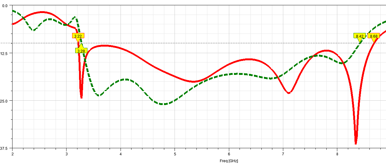
1698568061855.png


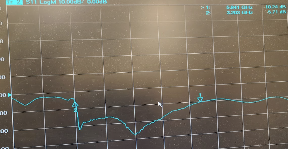
And, after the second fabrication, please see my second image, though the lower frequecy region is good, but the upper frequency region is going above the -10DB. Why the fabricated one is doesn't match well with my simulation. It's FR4 substrate.
1698568219496.png
 
Why the fabricated one is doesn't match well with my simulation. It's FR4 substrate.
Have you done tolerance analysis? FR4 permittivity can vary a lot, you should simulate from eps_r 4.0 to eps_r 4.8 and see how your results change.

Also, if you have small gaps or small conductor width, did you measure the actual dimensions in your hardware?

Regarding measurement, did you check VNA calibration? Did you check connector<> PCB transition using a simple structure like PCB thru line?
 
Would be instructive to know about antenna type. If the antenna has single ended feed line, cable waves are a popular cause of deviation from ideal antenna.
 
I see that the frequency response of the S11 measurement is not far from the frequency response of the optimized S11 simulation.
But the measured S11 magnitude is in average lower with about 5dB than the S11 magnitude of the optimized simulation shape.

Usually when have Er (permittivity) variations you get frequency shift of the S11 shape, and when have Loss Tangent variations, the magnitude of S11 will vary.
For example, if Loss Tangent vary from 0.02 to 0.01 you may get about 5dB magnitude variation of S11.
 
Have you done tolerance analysis? FR4 permittivity can vary a lot, you should simulate from eps_r 4.0 to eps_r 4.8 and see how your results change.

Also, if you have small gaps or small conductor width, did you measure the actual dimensions in your hardware?

Regarding measurement, did you check VNA calibration? Did you check connector<> PCB transition using a simple structure like PCB thru line?
VNA Calibration is fine. Double checked it. The connector is just a sma connector. Also checked that one. Well, I will check the permittivity and the actual dimension in the hardware.
--- Updated ---

I see that the frequency response of the S11 measurement is not far from the frequency response of the optimized S11 simulation.
But the measured S11 magnitude is in average lower with about 5dB than the S11 magnitude of the optimized simulation shape.

Usually when have Er (permittivity) variations you get frequency shift of the S11 shape, and when have Loss Tangent variations, the magnitude of S11 will vary.
For example, if Loss Tangent vary from 0.02 to 0.01 you may get about 5dB magnitude variation of S11.
How can I check this in actual hardware? Is there any way?
--- Updated ---

What environment do you use for antenna measurements ?
It is a general open environment, calibrating the VNA and measuring the response of the antenna.
--- Updated ---

Would be instructive to know about antenna type. If the antenna has single ended feed line, cable waves are a popular cause of deviation from ideal antenna.
Yes, it's a single feed line. I checked the cable and connector also. It is fine.
 
Yes, it's a single feed line. I checked the cable and connector also. It is fine.
I was asking about possible cable waves (cable becomes part of the antenna), not bad cable connection. We didn't yet see the antenna geometry, thus it's impossible to guess if cable waves are likely. There's however a simple test: Does S11 curve change when you enclose the cable with your hand? If so, you have a problem and should consider common mode isolation means for VNA test.

Several possible explanations for mismatch have been suggested, as far as reported here, you didn't yet check all of it. Repeating the simulation with different Er (and also different loss factor) should give you an overview how much the result depends on material variations.

At the end, S21 and directional characteristic matters for an antenna, S11 unfortunately doesn't distinguish between losses and radiation efficiency. In so far, S11 magnitude match shouldn't be overestimated.
 
The connector is just a sma connector. Also checked that one.

I am working in EM support (other tools, not HFSS) and have worked with customers on many of these "maesurement does not match simulation" cases. This requires a lot of attention to the detail, really!

At your working frequency, there are many possible issues with SMA PCB transition: cheap connectors, gap between PCB ground and SMA body, inappropriate soldering, inappropriate design of pads on PCB.

For example, a tiny gap can have a large effect by introducing series L.

serl.png
 
(cable becomes part of the antenna)
That's what I learned too when doing VNA measurements. Think of the outside of the shield and inside of the shield as 2 separate conductors, and they "touch" where you make the connection to your antenna. I've done this type of measurement in the past and I put a ferrite bead around the cable as close as possible to the connector, not sure if this helps, I was just going by what other people said.
 

LaTeX Commands Quick-Menu:

Part and Inventory Search

Welcome to EDABoard.com

Sponsor

Back
Top