Continue to Site

Welcome to EDAboard.com

Welcome to our site! EDAboard.com is an international Electronics Discussion Forum focused on EDA software, circuits, schematics, books, theory, papers, asic, pld, 8051, DSP, Network, RF, Analog Design, PCB, Service Manuals... and a whole lot more! To participate you need to register. Registration is free. Click here to register now.

Why M2 acts as a common gate stage in this circuit?

Status
Not open for further replies.

Osawa_Odessa

Banned
Joined
Dec 31, 2012
Messages
168
Helped
1
Reputation
2
Reaction score
1
Trophy points
1,298
Activity points
0
Hi,
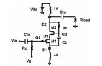
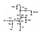
I want to analyse the circuit below. It is an RF power amplifier.
96832d1380548111-cascode.jpg

In DC mode:
Assuming that Ld is ideal then there is no DC voltage drop across it. => VD2 = VDD.
In the mean time, the capacitor is open at DC => no current flowing through Rb => VG2 = VD2 = VDD
In AC mode:
This is where I am confused. It is said that M2 acts as common gate here. This means that the gate of M2, G2, have to be connected to ground in AC mode, right?
But how can that be possible when there is the presence of Cb and Ls?
The voltage at gate of M2, VG2, will be equal to the total voltage across Cb and Ls. But VG2 is impossible zero, right?
And if so how M2 can be a common gate stage? Please explain? Thanks.
 

Attachments

  • Cascode.JPG
    Cascode.JPG
    16.6 KB · Views: 126

Confusion about RF ground

Hi, I am studying power amplifier from a paper.
Here is a circuit and some description about it.
attachment.php

A conventional cascode amplifier is shown in Fig. 1(a). Transistor M1 acts as a common source (CS) and transistor M2 acts as a common gate (CG). The RF signal is applied to G1. Gate, G2 is RF grounded with a dc value of Vdc which can be equal to the supply voltage Vdd . The RF ground at G2 can be achieved by either an off-chip or an on-chip capacitance resonating with the bond-wire inductance. The dc voltage at D2 is equal to the supply voltage with an RF voltage swing around this value.

There seems contradiction here.
1. Gate, G2 is RF grounded with a dc value of V which can be equal to the supply voltage Vdd.
2. The RF ground at G2 can be achieved by either an off-chip or an on-chip capacitance resonating with the bond-wire inductance.

G2 is directly connected to Vdd and therefore, at RF it is always ground, no need to use capacitance to resonate with the bond-wire inductance, right?
I think it is mistaken here. #2 should be "The RF ground at S1 can be achieved by either an off-chip or an on-chip capacitance resonating with the bond-wire inductance."

Do you think so? Thanks.
 

Attachments

  • Cascode 1.JPG
    Cascode 1.JPG
    17 KB · Views: 142
Last edited:

Why M1 has smaller drain-gate voltage swing than M2?

Hi,
Please explain why M1 has smaller drain-gate voltage swing than M2.
96835d1380643702-cascode-1.jpg

Here is description from the paper but I don't understand.
A conventional cascode amplifier is shown in Fig. 1(a). Transistor M1 acts as a common source (CS) and transistor M2 acts as a common gate (CG). The RF signal is applied to G1. Gate, G2 is RF grounded with a dc value of Vdc which can be equal to the supply voltage V . The RF ground at G2 can be achieved by either an off-chip or an on-chip capacitance resonating with the bond-wire inductance. The dc voltage at D2 is equal to the supply voltage with an RF voltage swing around this value. At maximum output power, the voltage at D2 swings down close to zero and up to twice V . In order to increase the efficiency, the voltage can be shaped by the choice of the matching network. In the cascode configuration, transistor M1 has a smaller drain–gate voltage swing. This is because the voltage at D1 is always lower than voltage at G2 by an amount equal to the gate–source voltage of G2. Consequently, the supply voltage is limited by the breakdown voltage of M2 rather than M1.

Why M1 has smaller drain-gate voltage swing than M2?
Answer:
"This is because the voltage at D1 is always lower than voltage at G2 by an amount equal to the gate–source voltage of G2. Consequently, the supply voltage is limited by the breakdown voltage of M2 rather than M1."
I am really not satisfied with the answer. Is there something obvious here that I don't know, please tell me?
And can you answer the question? Thanks.
 

Anyone helps? I didn't want to ask many questions in one thread like this. But the moderator has merged all of them into this thread.
 

Status
Not open for further replies.

Part and Inventory Search

Welcome to EDABoard.com

Sponsor

Back
Top