Continue to Site

Welcome to EDAboard.com

Welcome to our site! EDAboard.com is an international Electronics Discussion Forum focused on EDA software, circuits, schematics, books, theory, papers, asic, pld, 8051, DSP, Network, RF, Analog Design, PCB, Service Manuals... and a whole lot more! To participate you need to register. Registration is free. Click here to register now.

[SOLVED] Why there is a difference in the ADS layout and schematic simulation results?

Status
Not open for further replies.

Nathan1

Junior Member level 3
Joined
Jun 10, 2021
Messages
27
Helped
0
Reputation
0
Reaction score
0
Trophy points
1
Activity points
207
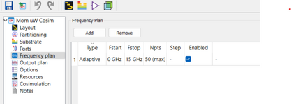
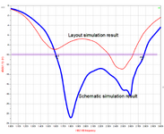
I am working on a rectifier. There is a difference in the layout and schematic simulated result (S11 plot attached). I know that the layout result usually differs from the schematic. Is it normal to have this much of a difference in the S11 plot as in the screenshot attached? The layout simulation result can be improved, but I'll do it once it's confirmed by someone that my EM setup is correct (ports settings, etc).

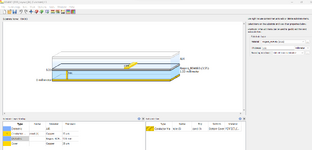
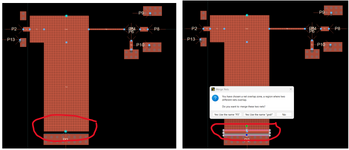
I have used TML for the input port as mentioned by volker@muehlhaus in his posts. Also used TML for the output port.

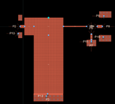
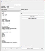
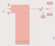
Dimensions of the Tlines and stubs are the same in schematic and layout. I have attached the layout, substrate (for both layout and schematic) and ports screenshot. Please have a look.

Thanks a lot.
 

Attachments

  • em frequency.png
    em frequency.png
    45.6 KB · Views: 85
  • layout substrate.png
    layout substrate.png
    61.6 KB · Views: 87
  • layout.png
    layout.png
    52.5 KB · Views: 86
  • performance comparison.png
    performance comparison.png
    91.2 KB · Views: 82
  • Schematic substrate.png
    Schematic substrate.png
    112.7 KB · Views: 79
  • cosim.png
    cosim.png
    39.7 KB · Views: 94

You have very different widths in TEE-junctions and large steps in width. Circuit models are not very accurate for these extreme dimensions. In this case, EM can be more accurate.
 
Last edited:
You have very different widths in TEE-junctions and large steps in width. Circuit models are not very accurate for these extreme dimensions. In this case, EM can be more accurate.
Thanks a lot, volker@muehlhaus. EM setup (ports setting) etc I have shared are fine, I guess?
 

EM setup (ports setting) etc I have shared are fine, I guess?
This is difficult to answer from the incomplete screenshots that you showed. You have placed some ports (P3, P12) and ground symbols near the vias that look strange to me.
 
This is difficult to answer from the incomplete screenshots that you showed. You have placed some ports (P3, P12) and ground symbols near the vias that look strange to me.
Thanks a lot, volker@muehlhaus. There was an extra gnd symbol I removed. The attached screenshot shows how I got gnd symbol. To further assess whether my setup is appropriate, I would like to share anything else you may need to know? I really appreciate your help.
 

Attachments

  • sss.png
    sss.png
    211.1 KB · Views: 75
  • ports.png
    ports.png
    120.3 KB · Views: 79

Thanks a lot, @BigBoss. I used ViaGnd it seems better. As shown in the screenshots above, do I still need to ground the short stub manually? In the schematic, we can't connect via to a short stub.
 

It's easy to connect a VIA to a component. Check the connections physically.
Simulation results should be very close. 
1692288122165.png


1692287988719.png


1692287139620.png
 
Last edited:
As shown in the screenshots above, do I still need to ground the short stub manually?
Placing the ground symbol has an effect for schematic simulation, but it has zero effect for layouts simulated in EM. The EM solution is based only on physical elements drawn in layout.

This means the ground symbol placed in layout at P13 etc is useless and misleading. Current in the EM model will flow through the two physical vias that you have drawn there.

gndsymbol.png
 

Yeah, that's it. You don't have to use shorted stub.
I don't like this approach. As you can see, the notches in S21 are off by more than 10%. This is due to the incorrect modelling of length at the shorted end when placing vias into the line.
 
I don't like this approach. As you can see, the notches in S21 are off by more than 10%. This is due to the incorrect modelling of length at the shorted end when placing vias into the line.
VIAs are not placed into the Line, they are attached to the Line. They seem to be but not true.
You're somehow right because VIAs' copper pours extend the TL's length.
1692373129113.png

If I place an alongside thin VIA at the end of the TL, the difference is very minor.
1692373694369.png

1692373712791.png
 

Status
Not open for further replies.

Part and Inventory Search

Welcome to EDABoard.com

Sponsor

Back
Top