Continue to Site
Follow along with the video below to see how to install our site as a web app on your home screen.
Note: This feature may not be available in some browsers.
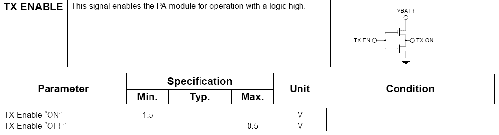
mjayanthr said:well it's a cmos inverter
if the upper transistor is p-channel
and the lower transistor is n-channel
Added after 25 seconds:
ya,.....well it's a cmos inverter
if the upper transistor is p-channel
and the lower transistor is n-channel
rfzheng said:if they are both n-channel, I have never see this type of source follower before, i think there must be very big leakage current.
but bow about upper nmos ,and lower pmos, there is a interviewer who asked me this question before.
hehe, is it funny? can you draw the output curve when the input voltage sweep from 0 to vbat??
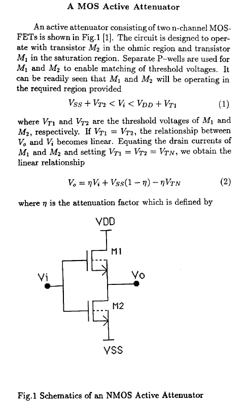
patriot said:It may be an active attenuator,I find a paper about this.
However,Vin is so small,why it need attenuation ?
If Vin<Vt,what's the voltage of Vout?
patriot said:from Razavi's book "Design of analog cmos",the bottom nmos is also saturated,
It is said that this source follower will have lower leakage current than the circuit which is followed by a resistor Rs?
However,according to the voltage Vin,Vbatt,the bottom nmos is in triode as amriths04 said.
PS:0<Vin<2V,Vbatt=3.5V
amriths04 said:what do you mean patriot?
why not?
if vth=1v and say you give a 0.5 v input, surely both transistors are going to be in cutt-off. so the output will be in a high impedance state. what is wrong with the above statement?