Welcome to our site! EDAboard.com is an international Electronics Discussion Forum focused on EDA software, circuits, schematics, books, theory, papers, asic, pld, 8051, DSP, Network, RF, Analog Design, PCB, Service Manuals... and a whole lot more! To participate you need to register. Registration is free. Click here to register now.
It looks oddly familiar to old Tek scope probe compensation for coaxial wire and shield inductance.
I tried to simulate it but not specified is the probe impedance or load.
This is what got without the DC rectifier for NET 1 and "guess-timating" White Box Rin = 1M showing -9 dB with break points at up 45 kHz and flat after 100 kHz.
Without more info, that's my best guess. It looks like it is designed for 0 ohm probes with twisted pair.
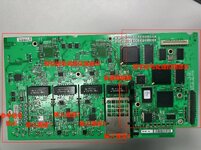
Attachment is a picture of the board. I can't find the model #. If you need the model #, I will try to find it.
This should be a very old TEK oscilloscope.
My oscilloscope is vintage Tektronix RM504. The instruction manual shows many RC networks used in various places. Sometimes there's a potentiometer in place of the resistance.
One function is called 'high-frequency compensation'. The capacitor is in parallel with a pot. Adjusting it changes the shape of a leading edge formed by the beam. We can adjust it so a waveform onscreen can have sharp attack or soft attack. The aim is to stay true to the signal. My impression is that the scope's circuitry tends to attenuate high frequencies, therefore any signal goes through series capacitors which serve as high pass filters.
My analysis: Other than guessed in post #3, the RC circuit isn't a voltage divider but a divider plus possibly feedback network of the input amplifier U1201. NET2 and NET3 represent input and possibly feedback output of the amplifier. Respectively it's difficult to make assumptions about its transfer function without knowing amplifier characteristic.
High impedance (1 MOhm input) dividers with 100 or more MHz bandwidth are always compensated RC parallel circuits.
The schematic seems either incomplete or incorrect. According to type code, K1200 is a bridge rectifier. But there should be a solid state relays shorting the input coupling capacitor.
The intent is to equalize a flat frequency response for a 10:1 or 1:1 probe, beyond tuning than the leadscrew trim cap on the probe to match the scope Zin.
Normally this is in the range of 50MHz to 500 MHz and not 100 kHz as my plot assumed for Net terminations.
Hi, FvM and Other Gurus,
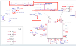
here is the SCH more precisely.
The U1201 is marked code as "9857-00", Package QFN52.
I searched and found it should be a product of NS, but can't find its datasheet.
May you comment on the NET2 and NET3 function?
Thanks.
Best,
Tony Liu
Hi, Yes, I know it.
I am curious about what the functions of the net2 block and the net3 block are.
Does anyone have datasheet for: The U1201 is marked code as "9857-00", Package QFN52. ?
This site uses cookies to help personalise content, tailor your experience and to keep you logged in if you register.
By continuing to use this site, you are consenting to our use of cookies.