Welcome to our site! EDAboard.com is an international Electronics Discussion Forum focused on EDA software, circuits, schematics, books, theory, papers, asic, pld, 8051, DSP, Network, RF, Analog Design, PCB, Service Manuals... and a whole lot more! To participate you need to register. Registration is free. Click here to register now.
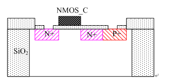
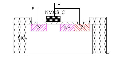
I think that this NMOS are connect bad because source is floating. If can be connect like diode, anode must be connect on higher potential, anode is P type. If can be connect like capacitor, drain and source must be connect on gate. In this case I think that it could be something like capacitor.
when the GATE connect the bulk
i think the device can be consider the two serial PN doides the voltage of the gate can control the current of the diode
This site uses cookies to help personalise content, tailor your experience and to keep you logged in if you register.
By continuing to use this site, you are consenting to our use of cookies.