Continue to Site

Welcome to EDAboard.com

Welcome to our site! EDAboard.com is an international Electronics Discussion Forum focused on EDA software, circuits, schematics, books, theory, papers, asic, pld, 8051, DSP, Network, RF, Analog Design, PCB, Service Manuals... and a whole lot more! To participate you need to register. Registration is free. Click here to register now.

What is port Z0 given by HFSS?

Status
Not open for further replies.

arve9066

Member level 2
Joined
Jan 21, 2016
Messages
48
Helped
0
Reputation
0
Reaction score
0
Trophy points
6
Activity points
446
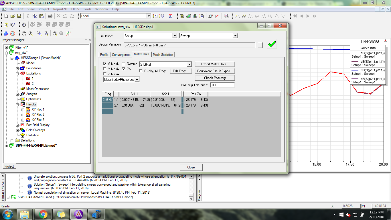
I am trying to simulate a rectangular waveguide and find out the characteristic impedance. What is the port Zo which is given in the Matrix data? Is it the same as characteristic impedance. Is there a scaling factor that I am missing?


port Z0 is the characteristic impedance of the structure. In order to find the correct value of Z0 take care that renormalize to 50 ohm check box isn't checked.
 

yea.. I am exciting only TE10 mode and the field plots confirm that. for the dimensions and frequency i hve chosen i should get 270 odd ohms where as i see 26.179 ohm.. this is where i m getting confused..
 

There are a few strange things I notice in your attached image - is b (= 39.5 mm) the width of your SIW? Using a dielectric constant constant with FR-4 = 4.4, the cutoff frequency should be 1.8 GHz, so I guess the mode should be supported at 2 GHz. I'm not sure why the characteristic impedance would have such a large imaginary component (~10 degrees?). Can you post some more information, such as the setup and scattering parameters, or perhaps attach the file?
 

There are a few strange things I notice in your attached image - is b (= 39.5 mm) the width of your SIW? Using a dielectric constant constant with FR-4 = 4.4, the cutoff frequency should be 1.8 GHz, so I guess the mode should be supported at 2 GHz. I'm not sure why the characteristic impedance would have such a large imaginary component (~10 degrees?). Can you post some more information, such as the setup and scattering parameters, or perhaps attach the file?

The SIW filter has a =53.74mm which corresponds to a cutoff of 1.5GHz with a Rogers 4350 substrate of dielectric constant 3.66. Please find attached the hfss design file. It is a 3rd order chebyshev iris filter that I am trying to design. I get the filter response, but I am not able to undersdtand what the port Z0 is
 

Attachments

  • Filter_v1.zip
    93 KB · Views: 176

Hi arve9066,

Your simulation setup, as well as the results, seem to be correct.

Characteristic impedance is not uniquely defined for non-TEM modes -- many textbooks will use the "wave impedance" definition, however, this doens't take into account the geometrical parameters of the waveguide (which HFSS does). To convert between the two, simply multiply the HFSS result by a/b.
 
That's something I did not know. Thanks for that information. Is there anywhere in the HFSS documentation I could find this?

At 2GHz which is above the cutoff frequency, the port Z0 given by HFSS is 3.96. Multiplying with a/b (53.74/0.6) gives me 350 ohms around. For an equivalent rectangular waveguide filled with dielectric of er=3.6 is, I remember I should ve got around 270 ohms.
 

So when I calculate the Z parameters from solution data, they are normalized to the Z0 which is the port Z0 displayed HFSS times (a/b). Am I correct?
 

That's something I did not know. Thanks for that information. Is there anywhere in the HFSS documentation I could find this?

At 2GHz which is above the cutoff frequency, the port Z0 given by HFSS is 3.96. Multiplying with a/b (53.74/0.6) gives me 350 ohms around. For an equivalent rectangular waveguide filled with dielectric of er=3.6 is, I remember I should ve got around 270 ohms.

There's more ambiguity still to come. The way in which characteristic impedance is calculated for non-TEM modes can also vary depending on your choice of equivalent "voltage", "current", or power. Search the documentation for "Calculating Characteristic Impedance". Unfortunately, I don't think there's any documentation on the various plane-wave or other definitions. This isn't really talked about much, even in the literature...

So when I calculate the Z parameters from solution data, they are normalized to the Z0 which is the port Z0 displayed HFSS times (a/b). Am I correct?

Yes, converting from S to Z parameters requires using the characteristic impedance values.
 
Hello
what is antenna input impedance variable in HFSS? Terminal Port Z0 or Terminal Z parameters?
Thanks
 

input impedance in a one port network is Z11.
 

Thank you
So for a helical antenna with axial mode this input impedance is acceptable for a range of frequencies?because in a reference it mentioned that helical antenna input impedance is approximately between 150-300 ohm
ante.jpg
 

you should see the real and imaginary part instead of magnitude. For the antenna to be matched, the real part should be around 50 ohms and the imaginary part near zero.
 
  • Like
Reactions: baby_1

    baby_1

    Points: 2
    Helpful Answer Positive Rating
For the antenna to be matched, the real part should be around 50 ohms and the imaginary part near zero.

If you're planning on matching to 50 Ohms. I don't believe a reference impedance was specified. Many legacy antenna systems use a "system" impedance of 75 or even 300 Ohms.

baby_1, "impedance bandwidth" is usually observed via scattering parameters or VSWR -- it's a bit hard to gauge performance by direct observation of (the magnitude of) input impedance.
 
  • Like
Reactions: baby_1

    baby_1

    Points: 2
    Helpful Answer Positive Rating
Thanks you PlanarMetamaterials
what do you mean about "t's a bit hard to gauge performance by direct observation of (the magnitude of) input impedance"?
because as I know we can treat identical to Input impedance and S parameters and both of them can give us input impedance but in real sometimes input impedance is to hard to measure but s parameters are fine.However in simulation , are they different?or have any advantages?
 

Nothing's wrong with the data; it's just not what we're used to seeing in antennas. I'm usually always looking at S-Parameters in dB, so looking at input impedance is a bit foreign. You also left us assuming the characteristic "system" impedance that you're matching to -- is it 50 ohms or something else?
 
  • Like
Reactions: baby_1

    baby_1

    Points: 2
    Helpful Answer Positive Rating
The filter was designed with a center frequency of 2GHz with 200MHz bandwidth. I get acceptable performance at this range. But there is equally good s21/s11 characteristics at higher frequencies too. If you simulate the filter you will notice it. Is it inherent for waveguide cavity filters that a TE102 mode is excited anyways with TE101 mode? What is a way to get around it?
 

Status
Not open for further replies.

Part and Inventory Search

Welcome to EDABoard.com

Sponsor

Back
Top