Continue to Site

Welcome to EDAboard.com

Welcome to our site! EDAboard.com is an international Electronics Discussion Forum focused on EDA software, circuits, schematics, books, theory, papers, asic, pld, 8051, DSP, Network, RF, Analog Design, PCB, Service Manuals... and a whole lot more! To participate you need to register. Registration is free. Click here to register now.

What IC inside thi sintegrated module?

Status
Not open for further replies.

TekUT

Full Member level 6
Joined
Jun 17, 2008
Messages
323
Helped
39
Reputation
78
Reaction score
15
Trophy points
1,298
Location
Italy
Activity points
3,557
What IC inside this integrated module?

Dear all,
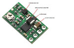
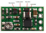
I'd like to ask if someone know what type of switching controller was used inside this integrated module (SEPIC topology, 1.5 MHz switching frequency), here below the general specification:

Min. input voltage: 1.5 V
Max. input voltage: 16 V
Min. output voltage: 2 V
Max. output voltage: 12 V
Continuous output current: 300 mA (max)
Integrated over-temperature protection
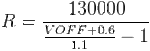
shutdown threshold can be programmed by using the relation show into the file equation.gif attached.

About the module name you can look at the "module-name.jpg" image attached.

I've did a search from Nation, LT, Intersil and so on but I'm unable to find a controller able to fit this data, I'm gratefully if someone have some idea regarding it.

Thanks in advance
Pow
 

Attachments

  • equation.gif
    equation.gif
    946 bytes · Views: 99
  • module-name.jpg
    module-name.jpg
    29.6 KB · Views: 106
Last edited:

Dear All,
after some surfing may be I've found the IC, actually it's seems close to the SEMTECH model SC4502:

https://www.semtech.com/images/datasheet/sc4502.pdf

If we set a 0.6 V hysteresis for the shutdown circuitry, by using the (11) at page 11 we obtain:

R3=VHYS/IHYS=0.6/4.6uA=130434.78 ohm then 130000 ohm

by using the equation (12) we can obtain the R4 value as:

R4=130000/((VH/1.1)-1)

using the (10) we can evaluate VH as:

VH=VL+VHYS=VL+0.6

then the design equation for R4 will be:

R4=130000/((VL+0.6)/1.1 - 1)

which is exactly the equation reported into the "equation.gif" image file attached when you rename VL to VOFF.

What is your point of view, may be this one the device?

Thanks again for your attention.

Bye
Pow
 

You have to lookout for a SEPIC rather than BOOST converter IC!
 

Dear FvM,
yes I know that because the output should be high or below the input voltage and also because the original module claim it a s a SEPIC but I've did some search also into this direction without found anything with same package and input voltage range, the only chip that seems to meet this requirement is like the SC4502. Also if you look at page 16 into the device datasheet at figure 11 there is an application circuit regarding the SEPIC topology with this IC. This was the hook that give me that the used IC should be the SC4502, but of course I'm not sure 100%, do you have some idea where to look in order to get a final answer to this question?

Here in attachement some idea that inspire me about SEPIC.


Thanks for your time!

Best regards
Pow
 

Attachments

  • Component.jpg
    Component.jpg
    97.1 KB · Views: 90
Last edited:

Yes, I didn't consider the option to operate a boost converter in SEPIC mode. I agree, that your consideration sounds plausible.
 

Yes, I didn't consider the option to operate a boost converter in SEPIC mode. I agree, that your consideration sounds plausible.

I've revised the component identification because the inductor connector from the anode of the output diode and ground have a footprint with just two pad then it seems more likely a single inductor than a coupled one.

Following this I've thinked a new disposal reported into the attached image, now to be sure about this new one I've to make some design in order to see what are the feasible value for L1 and L2.

Into this application notes:

https://smd.hu/Data/Cooper/Pdfs/Inductor SEPIC App Notes.pdf

I can read at the bottom right of the page 1:

"Using the nearest preferred value would lead to the selection of a 22 μH inductor. It is common practice to select the same value for both input and output inductors in SEPIC designs although when two separate parts are being used it is not essential."

then may be the two inductor on the board will be set with different value then the reason why the two footprint are different.

What are your think about this new assumption?

Thanks again.

Reagrds
Pow
 

Attachments

  • Component-hypothesis-2.jpg
    Component-hypothesis-2.jpg
    94.1 KB · Views: 110
Last edited:

Status
Not open for further replies.

Similar threads

Part and Inventory Search

Welcome to EDABoard.com

Sponsor

Back
Top