Continue to Site

Welcome to EDAboard.com

Welcome to our site! EDAboard.com is an international Electronics Discussion Forum focused on EDA software, circuits, schematics, books, theory, papers, asic, pld, 8051, DSP, Network, RF, Analog Design, PCB, Service Manuals... and a whole lot more! To participate you need to register. Registration is free. Click here to register now.

Regarding PSFB Evaluation Module

sabu31

Advanced Member level 1
Joined
Jan 28, 2011
Messages
446
Helped
12
Reputation
24
Reaction score
13
Trophy points
1,298
Activity points
5,157
Dear All,

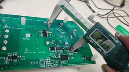
I am studying PCB of the PSFB evaluation board from TI.

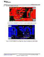
One thing I want to know is the limit for gate trace length. Generally, we know that the gate trace should be short. But in this board its roughly 2 inches.

Also, the return path for the gate should connect to the ground plane a single point right instead of using a common ground plane. Is there any thing missing in my understanding.

The top switches are on the same heatsink and the bottom switches are on the same heat sink. Is there any particular benefit in this arrangement.
 

Attachments

  • Gate Trace Lenght.jpg
    Gate Trace Lenght.jpg
    104.5 KB · Views: 64
  • EVALUATION BOARD DOC_Page_21.png
    EVALUATION BOARD DOC_Page_21.png
    43.9 KB · Views: 62
  • EVALUATION BOARD DOC_Page_07.png
    EVALUATION BOARD DOC_Page_07.png
    87.3 KB · Views: 59
Gate trace can be as long as you still get an acceptable gate waveform. No general rule for trace length. Gate input capacitance, gate resistor, driver output rise/fall time matters, also trace width and enclosed loop area.

Also, the return path for the gate should connect to the ground plane a single point right instead of using a common ground plane. Is there any thing missing in my understanding.
You refer to low side drive? Are you suggesting to ground UCC27714 directly to low side source instead of PGND plane? I don't see an advantage, even if it would be feasible with present component placement. Consider that the probably largest parasitic effect in gate circuit is caused by source inductance of the three terminal package.
 
It is not so much the GD length - but the area inside the send and return traces

if this area is as small as can be practically made - then you can do no better - this is why a twisted pair of 3 inches is better than a 1 inch pcb trace with a 1 inch square area for send and return !

[ L = N^2 . Ae . Ur. Uo / mag path length ] so doubling the area = twice the L for the gate drive leads

you can chuck in a fine twisted pair ( in parallel ) to the extant circuit and see if the GD signals improve - it will not harm operation.
 
Last edited:
Since trace inductance on source to rail affects Vgs vs Id , it can resonate with Ciss, & may amplify load resonances. Knowing these series RLC parameters for Q and fo helps you understand if it contributes to ringing. with very fast risetime currents so generally Vs to gnd. plane on Nch is very short.

Use a 10:1 probe without gnd clip,and probe tip, only using a spring probe to eliminate all resonance > 20 MHz.
 
Last edited:
Is there any particular benefit of keeping the top switches on the same heatsink and bottom switches on same heatsink. Instead of commonly seen , one on one heat sink.
 
Is there any particular benefit of keeping the top switches on the same heatsink and bottom switches on same heatsink. Instead of commonly seen , one on one heat sink.
Yes. This will reduce crosstalk from Pch Id to Nch Vgs and visa versa
 
The top switches are on the same heatsink and the bottom switches are on the same heat sink. Is there any particular benefit in this arrangement.
Both heatsinks are connected to PWRGND, "hot" low side drains inject current through insulation pad capacitance. Current distribution would be different with different heatsink topology, but I won't expect a big effect. Or are you comparing to unisolated individual heatsinks?
 
Both heatsinks are connected to PWRGND, "hot" low side drains inject current through insulation pad capacitance. Current distribution would be different with different heatsink topology, but I won't expect a big effect. Or are you comparing to unisolated individual heatsinks?
I am comparing this a One Half Bridge Leg on a single heatsink to Top Switches on a Single Heatsink and Bottom Switches on the heatsink.

Also is grounding of Heatsink is generally done in SMPS. I mean suppose the DC link is say 1500V, then the only thing insulating the HV Terminal from the Ground is the heatsink insulator pad for the MOSFET.
 
Devices rated for 1500 V usually come in packages that allow respective insulation. The present circuit is designed for 390 V bus.

But generally speaking, common and grounded heatsink isn't optimal for all designs. In this case in has been probably chosen for simplicity and EMI properties.
 
I am making a PSFB converter based on based on the layout in the evaluation module.

I am however using TO 247 devices and slightly bigger heatsink. Is the layout acceptable for this primary side schematic . I have not included gate side and secondary side components. Need to confirm whether this layout in primary side is acceptable.

Also I want to confirm position for the primary side clamp diodes, whether it should be near the devices or the transformer

The input is 400V. Output 48. Power level 1500W . Switching frequency is 100kHz.

Please suggest any improvement in layout.
 

Attachments

  • PSFB_LAYOUT_PRIMARY_D.pdf
    19.2 KB · Views: 45
  • PSFB_Schematic_PRIMARY_D.pdf
    20.3 KB · Views: 52
I am making a PSFB converter based on based on the layout in the evaluation module.

I am however using TO 247 devices and slightly bigger heatsink. Is the layout acceptable for this primary side schematic . I have not included gate side and secondary side components. Need to confirm whether this layout in primary side is acceptable.

Also I want to confirm position for the primary side clamp diodes, whether it should be near the devices or the transformer

The input is 400V. Output 48. Power level 1500W . Switching frequency is 100kHz.

Please suggest any improvement in layout.
If you want to re-read my answer, to understand it, estimate the capacitance between each pin/pad to the heatsink, then add to your simulation.
 
There is only one reason to use a PSFB instead of a standard Full Bridge, and that is switching losses.
Turn on switching losses of a PSFB , which is reasonably loaded, will be near zero due to ZVS turn on.....so it doesnt matter if
you turn the fets on slow.
But..
The turn off switching losses of a PSFB can be very high indeed, and if you do not put a turn off sunubber on each fet, and turn the fets off lightning fast, then you are not really doing the PSFB
properly.
So you need a series diode in the gate drive so that you can slam the fets off super fast.....even a PNP turn off will not really turn them off as quick as you need...you really need a low Z
gate drive chip to slam the fets off quickly. So really you need
a hi side gate drive supply, and couple up to it with a Pulse transformer, or one of the digital isolators with sufficient
CMTI. And also a good negative withstand voltage on the switching node that gets connected to your "isolator chip". This wont mean any more room on the pcb, since it will mean your heatsink can be smaller.

If you are doing 1kw+, and you are not doing it like this, then you are wasting your money....but having said that, many who do 1kw+ SMPS with a plain full bridge and 20khz, and slow on/off fets, and quite large product, which they are happy with, would disagree with me, and i take my hat off to the "1kW/+20kHz" fraternity. I mean, the 20khz, 1kw+ full bridge can end up being nice and cheap.

BTW, if you do add biggish caps on VDs of fets, then best you do turn them on slowly--ish
 
Last edited:

LaTeX Commands Quick-Menu:

Similar threads

Part and Inventory Search

Welcome to EDABoard.com

Sponsor

Back
Top