Continue to Site

Welcome to EDAboard.com

Welcome to our site! EDAboard.com is an international Electronics Discussion Forum focused on EDA software, circuits, schematics, books, theory, papers, asic, pld, 8051, DSP, Network, RF, Analog Design, PCB, Service Manuals... and a whole lot more! To participate you need to register. Registration is free. Click here to register now.

Voltage route consideration

Status
Not open for further replies.

vijaymishra

Newbie level 5
Joined
Jun 8, 2009
Messages
8
Helped
1
Reputation
2
Reaction score
1
Trophy points
1,283
Activity points
1,333
Hi,
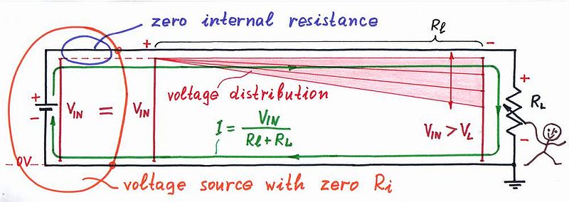
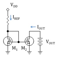
I case of a current mirror layout, the gate voltage line is under consideration. We are required not to route voltage lines for long.
As per my understanding, the RC model [per suqare] of the metal track, acts like a RC network for the voltage source [Vgs].Depending on the RC time constant, it will charge and will tranfer the voltage to the next cap. Hence the voltage at the end of the line will be the same Vgs as that at the source. So what is the exact reason to keep the voltage route to minimum?
 

Hi reason behind the minimum trace length is reduce the voltage drop and get the maximum supply input to required device.
Regards
Praveen Bhat
 

Hi, Thanks for the reply. The question is how is the voltage drop happening? Whatever current flows for the small time duration to charge the capacitor results in the capacitor voltage reaching to Vg. So how is the drop happening?
 

Hey friend trace is nothing but copper...what is copper copper..every path is work as a resistor..what is resistor..?
which will resist the flow of electron..ultimately voltage drop happens..and you are not using only trace..pcb board made up off some conducting material (FR4)
it has its own effect..

Regards
Praveen Bhat
 

Thanks again. But i disgree that every path is just R. Any metal trace is an RC network and not just R. Had they been just R network, then yes there would have been voltage drop which can be significant to ruin the design. Practically this is not the case. So the question remains the same, how is the drop happening?
 

A current flowing through the non-zero resistance of a practical conductor necessarily produces a voltage across that conductor. The dc resistance of the conductor depends upon the conductor's length, cross-sectional area, type of material, and temperature.
The local voltages along a long line decrease gradually from the source to the load

If the voltage between the conductor and a fixed reference point is measured at many points along the conductor, the measured voltage will decrease gradually toward the load. As the current passes through a longer and longer conductor, more and more of the voltage is "lost" (unavailable to the load), due to the voltage drop developed across the resistance of the conductor. In this diagram the voltage drop along the conductor is represented by the shaded area. The local voltages along the line decrease gradually from the source to the load. If the load current increases, the voltage drop in the supply conductor also increases. Voltage drop exists in both supply and return wires of a circuit.
 

The question is more with respect to the MOS current mirror and not with any other route. The voltage route in consideration is the the metal track connecting the gates of the mosfets in a current mirror. With this scenario the above explanation does not hold good.

---------- Post added at 11:20 ---------- Previous post was at 11:19 ----------

98_1299666007.jpg
 

The problem is more with the current mirror matching rather than routing.
When you have your 2 transistors far away from each other, you will not expect transistors to match and hence lousy mirroring.
Hence, it is always recommended to use voltage-mode bias distribution locally, and current-mode bias distribution globally.

The only routing dependent aspect I can think of is capacitive coupling of noise onto this bias voltage from other circuits.
 

Consider the case of a mirror rack similar to what
you show, or perhaps larger in number of mirror
outputs and having some physical extent. Bearing
in mind that as far as LVS is concerned, you can
attach the input current to the gate trace anywhere
you like.

If the active shunt is at the point where the reference
current enters the "rack" then all the rest of the gate
line has only AC current induced I*R deflection.

If you were to inject the current at the other end
then there would be some DC debiasing along the line
and this would be a systematic error (likely small, but
professors like to pick on small problems for purposes
of illustration).
 

Thanks for the reply. As this gate route [in metal] increases in its length, there would be voltage drop on the line. What equations will model the voltage drop in the metal path? There should not be a current flow in a voltage path. Is this correct?
 

There is current (Ids) in the master FET. You would like this to
not involve the gate or source routing of the others. Think "star
ground".
 

Thanks for the reply. As this gate route [in metal] increases in its length, there would be voltage drop on the line. What equations will model the voltage drop in the metal path? There should not be a current flow in a voltage path. Is this correct?

As checkmate already pointed out two major points to keep mirroring devices close are
- device mismatch (e.g. difference in Vth)
- gate voltage noise (crosstalk into the bias line will take longer to resolve when there is a higher RC load to the bias source)
In addition there is
- source voltage (ground or supply) correlation (which deteriorates with distance)

As of you questions, there is no relevant DC current in the bias line (unless you are using ultradeep submicron gates and a number of them). Crosstalk though can induce AC currents that will try to re-establish the perturbated bias voltage.
If you want to have a simple model of this, you can imagine an aggressor line capacitively coupled to your bias line. A voltage step on the aggressor line induces a certain amount of charge across the coupling cap, this charge will have to be absorbed by the bias generator gm across the bias wiring RC network...

Hope this helps
 

Status
Not open for further replies.

Part and Inventory Search

Welcome to EDABoard.com

Sponsor

Back
Top