Continue to Site

Welcome to EDAboard.com

Welcome to our site! EDAboard.com is an international Electronics Discussion Forum focused on EDA software, circuits, schematics, books, theory, papers, asic, pld, 8051, DSP, Network, RF, Analog Design, PCB, Service Manuals... and a whole lot more! To participate you need to register. Registration is free. Click here to register now.

Voltage Multiplier/doubler? Help explain circuit operation

Status
Not open for further replies.

faisal78

Member level 3
Member level 3
Joined
Aug 27, 2004
Messages
62
Helped
0
Reputation
0
Reaction score
0
Trophy points
1,286
Visit site
Activity points
592
Hi
I was trying to figure out this circuit but could not figure out its operation.
I had done a simple simulation, it seemed to work as per intention, i.e. a DC voltage doubler/multiplier?..
Can somebody help me understand how it works and its circuit tradeoffs.

BTW - this is not the typical flying capacitor/switching diodes circuit. its only based on 2 BJT transistors.

Below are the schematic and the simulation results.
Essentially, the input (V1) is a voltage source from a DAC that can output from 0v - 4v.
The simulation results DC sweep on the x-axis is sweeping V1.
Output is monitored from C2 output cap.

As you can see from the results, once V1 exceed ~600mV which turns on Q1, the output starts to "double/triple" based on the input until saturation.
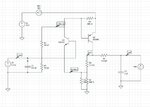
Schematic_Multiplier.JPG

DC_Sweep_Tune_multiplier.JPG
 

The graph indicates a gain of 3.2

The V1 is not needed if the input bias was changed with R1=640R then the 600 mV offset can be removed if R1C1 is detached from ground and used as an input.

I might've estimated the gain as the negative feedback ratio of Rc/Re=1.2k/0.34k=3.5

where 680R//680R = 0.34K


Hi, thanks for your replied, but I wanted to clarify something.
V1 is not intended for biasing.
It is the actual analog DAC voltage that is needed at the input of the circuit and being "multiplied" but the circuit.
 

When you provide a DC input, the circuit will provide ordinary voltage gain. (As you say, the input must be high enough to turn on Q1.)


This can be done with fewer components, however.

Then I wondered about the label 'tune' at the input. This suggests the input is supposed to be AC.

Could this be a frequency doubler?

I did some experimenting. I discovered it does work as a frequency doubler.

It requires (a) some amount of input resistance, (b) a resistor to load the output capacitor, and (c) careful adjustment of the bias current.


I would not be surprised if this was the schematic's intended function.
 

Nope. TUNE is definitely not AC input. It is a DC voltage from a DAC.
It looks like a frequency doubler just because the output voltage became saturated

When you provide a DC input, the circuit will provide ordinary voltage gain. (As you say, the input must be high enough to turn on Q1.)


This can be done with fewer components, however.

Then I wondered about the label 'tune' at the input. This suggests the input is supposed to be AC.

Could this be a frequency doubler?

I did some experimenting. I discovered it does work as a frequency doubler.

It requires (a) some amount of input resistance, (b) a resistor to load the output capacitor, and (c) careful adjustment of the bias current.


I would not be surprised if this was the schematic's intended function.
 

The graph indicates a gain of 3.2

The V1 is not needed if the input bias was changed with R1=640R then the 600 mV offset can be removed if R1C1 is detached from ground and used as an input.

I might've estimated the gain as the negative feedback ratio of Rc/Re=1.2k/0.34k=3.5

where 680R//680R = 0.34K

Let me summarize.

This is traditional 2 transistor negative feedback controlled-gain amplifier.

The low gain is due to the low impedance ratios Rc/Re
The input offset is the Vbe, which I advised how to improve.

Calling an amplifier a "multiplying" implies non-linear multiplication of 2 inputs.
Although gain is a multiple of input voltages, we refer this as simply a voltage amplifier to imply it is is intended to be a linear amplifier.

The huge gain of the 1st stage and 2nd stage is fed back to the emitter of Q1 as a common base feedback input, which is non-inverting, thus only 1 inverting stage in the feedback loop.

Many improvements can be made using a simple op Amp with much lower input offset, lower output impedance and higher input impedance.

But two stages has its limitations but for the purpose of amplifying a 3V DAC to >9V, it works.
 

Status
Not open for further replies.

Part and Inventory Search

Welcome to EDABoard.com

Sponsor

Back
Top