Continue to Site

Welcome to EDAboard.com

Welcome to our site! EDAboard.com is an international Electronics Discussion Forum focused on EDA software, circuits, schematics, books, theory, papers, asic, pld, 8051, DSP, Network, RF, Analog Design, PCB, Service Manuals... and a whole lot more! To participate you need to register. Registration is free. Click here to register now.

VLSI: active and n+/p+

Status
Not open for further replies.

yannik33

Member level 1
Joined
Oct 18, 2011
Messages
34
Helped
0
Reputation
0
Reaction score
0
Trophy points
1,286
Activity points
1,507
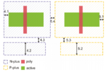
Why differentiate VLSI-Systems between active and n+ resp. p+ ? If the p+ region is larger doesn't this increase the likelihood of an short circuit between drain and source (eg in the figure below there is a connection between drain and source side doesn't this lead to a short circuit?)?
capture002.png
(**broken link removed** ,p. 7)
 

Yes, I think you are right: MOSFETs shouldn't be in a highly doped region, they must be in lowly doped regions, as p-substrate for NMOS or n-well for PMOS.

This p. 7 of the DRM.pdf is surely erroneous. Of course a highly doped region for contact to GND respective VDD should be close to the MOSFET's source (or such a bulk contact ring around the transistor(s)), but never over the MOSFETs itselves.
 

Poly and Field Oxide (= !active) are both hard-masks for
P+ and N+.

Many flows allow butted N+/P+, there is no good reason to
enforce a global spacing rule (other than they never tried
it, to say that it's fine). There are good reasons to butt
body and source regions, like device compactness of
3T layouts.
 

Status
Not open for further replies.

Similar threads

Part and Inventory Search

Welcome to EDABoard.com

Sponsor

Back
Top