Continue to Site

Welcome to EDAboard.com

Welcome to our site! EDAboard.com is an international Electronics Discussion Forum focused on EDA software, circuits, schematics, books, theory, papers, asic, pld, 8051, DSP, Network, RF, Analog Design, PCB, Service Manuals... and a whole lot more! To participate you need to register. Registration is free. Click here to register now.

[SOLVED] VHDL: Unknown post implementation behavior of signed fixed defined signals

Status
Not open for further replies.

zermelo

Junior Member level 3
Joined
May 24, 2013
Messages
25
Helped
0
Reputation
0
Reaction score
0
Trophy points
1,281
Activity points
1,543
Hi all,

I am working with a transceiver board to implement a Hamming windowed Chirp (linear frequency modulation) transmitter into a Cyclone II. Due to economic issues, instead of loading values into a DAC, we are using a dual MOSFET driven by complementary TTL signals to control the transformer stage (2 KVolts) that will drive a transducer.

I have done the VHDL coding , defined some I/O constraints and done the behavioral simulation. Everything works as specified in behavioral simulation : the two TTL have the correct timing, and are enabled a time which is proportional to the product of the window samples and the instantaneous frequency.

Long story short:

When I configure the board, and plug a TX trigger, both TTL signals remain stuck at zero. The Quartus Technology viewer says that the logic to generate them is in place.

Here is the VHDL related with the TTL signal generation:

Code:
-- P_TTL_GEN: TTL signals are gated with the result of the time interpolated unit
-- and the Hamming window readings.
P_TTL_GEN: process(i_clk)
begin
  if (i_clk'event and i_clk = '1') then 
    if (i_rst = '1') then 
      s_ttl_cnt_p <= (others => '0');
      s_ttl_cnt_n <= (others => '0');
      s_tx_n      <= '1';
      s_tx_p      <= '0'; 
      s_p_cnt_set <= '0'; 
      s_n_cnt_set <= '0'; 
    else
        
      -- tx_p generation  
      if (s_tx_cr_p_zc = '1') then -- Chirp sine rising edge
        s_ttl_cnt_p <= (others => '0');
        s_tx_p      <= '0';
        s_p_cnt_set <= '1';           
      elsif (s_p_cnt_set = '1') then  
        if (s_ttl_cnt_p < s_ttl_high) then   
          s_ttl_cnt_p <= s_ttl_cnt_p + 1;
          s_tx_p      <= '1'; 
        else
          s_p_cnt_set <= '0'; 
          s_tx_p      <= '0';
        end if;
      end if;         
      
      -- tx_n generation
      if (s_tx_cr_n_zc = '1') then -- Chirp sine falling edge
        s_ttl_cnt_n <= (others => '0');
        s_tx_n      <= '0';
        s_n_cnt_set <= '1';           
      elsif (s_n_cnt_set = '1') then  
        if (s_ttl_cnt_n < s_ttl_high) then    
          s_ttl_cnt_n <= s_ttl_cnt_n + 1;
          s_tx_n      <= '1'; 
        else
          s_n_cnt_set <= '0'; 
          s_tx_n      <= '0';
        end if;
      end if; 
        
           
    end if;
  end if;
  
end process P_TTL_GEN;

What I am afraid is that the logic for the comparison of the timer and the threshold value is implemented incorrectly. Those signals , s_ttl_cnt_n, s_ttl_cnt_p, s_ttl_high are defined as:

Code:
signal s_ttl_high  : unsigned(14 downto 0); 
signal s_ttl_cnt_n : unsigned(s_ttl_high'range);
signal s_ttl_cnt_p : unsigned(s_ttl_high'range);

The s_ttl_high signal is generated as:


Code:
-- P_TTL_HIGH: This product determines the % of TTL pulses within one 
-- period or the time that the PWM is high within one period.
P_TTL_HIGH: process(i_clk)
begin
  if (i_clk'event and i_clk = '1') then 
    if (i_rst = '1') then 
      s_ttl_high_sfx <= (others => '0');
    elsif (s_ttl_data_hi_rdy = '1') then
      s_ttl_high_sfx <= s_wdw_high_sfx*s_ttl_tunit_high_sfx ; 
    end if;
  end if;
end process P_TTL_HIGH; 


P_TTL_HIGH_CONV: PROCESS(i_clk)
begin
  if (i_clk'event and i_clk = '1') then 
    s_ttl_high <= to_unsigned(to_integer(s_ttl_high_sfx(s_ttl_high_sfx'left downto 0)),s_ttl_high'length);
  end if;
end process P_TTL_HIGH_CONV;

And s_ttl_high_sfx is a signed fixed defined as:

Code:
signal s_ttl_high_sfx : sfixed(13 downto -2);


I have done some debugging (unluckily I do not have direct JTAG acces to the FPGA, therefore I have no way to use signal tap for this) using testpoints, and observed that the zero crossing signals (s_tx_cr_p_zc and s_tx_cr_n_zc) and s_ttl_data_hi_rdy are generated generated correctly.

Do you see any problem in the conversion of P_TTL_HIGH_CONV? Could the comparison be failing due to that or any other reason? Any advice to debug this?

In the meantime I am trying to get a Cyclone development board so I can have acces to more signals and use Signal Tap.

Thanks in advance

Jose
 

Why is s_ttl_high defined as unsigned, when s_ttl_high_sfx is signed?
Your code is not illegal, and kind of should work. But any -ve values are actually a very large unsigned value, but I guess this is how it is supposed to work (if the signed is all 1s, then you need to count a long time before turning off s_tx_p/n).

Im not sure what the synthesisor is doing here. Because you can technically converting -ve values to unsigned, and this would cause a failure in simulation, Im not sure how the synthesisor is doing the conversion. But I would expect it to simply take the msbs of the sfixed

Just to be sure, try this instead (as it will pass in simulation):

s_ttl_high <= unsigned( to_signed(s_ttl_high_sfx(s_ttl_high_sfx'left downto 0)));
 

Why is s_ttl_high defined as unsigned, when s_ttl_high_sfx is signed?
Your code is not illegal, and kind of should work. But any -ve values are actually a very large unsigned value, but I guess this is how it is supposed to work (if the signed is all 1s, then you need to count a long time before turning off s_tx_p/n).

Hi Tricky. I remember you helped me out with a linear interpolator implementation some time ago. That s_ttl_high_sfx is the output of that interpolator, which I decided to implement as signed fixed for the purpuse of reusability.s_ttl_high is defined as unsigned because it has to be compared with the values of a timer.


Just to be sure, try this instead (as it will pass in simulation):

s_ttl_high <= unsigned( to_signed(s_ttl_high_sfx(s_ttl_high_sfx'left downto 0)));

I tried it and yes, simulation is ok, but I get the same result in the board. Just to make sure I tried other things:

1) I replaced the comparison with s_ttl_high for an unsigned value (450). That gives me a square wave in the complementary TTL outputs in the board, with the right frequency.

2) I measured s_ttl_high bit by bit with a single testpoint (needed 14 bitstreams:)). The result is all zeroes. At this point I do not understand Quartus, the RTL viewer and the Chip planner show the comparison logic. There are no inputs tied to 0 or strange things as far as I can see.

I am downloading Quartus 14 and will try with a Cyclone V board I got. But I only expect to see s_ttl_high tied to ground in Signal tap...

Thanks again
 

can you post the whole code? have you managed to get the s_ttl_high_sfx stuck at 0?

- - - Updated - - -

even better, post the project?
 
Hi,

Hmmm. As easy as that , I should be measuring s_ttl_high_sfx to see if the conversion is failing. The code and the FPGA project is propietary , its part of an R & D activity that will become a product later. I will check with management. In any case, I would send you the project to your email.

thanks!

Jose
 

Have you looked at the post synthesis viewer? Tracing the outputs back and seeing what the synthesis did might shed some light on the problem.
 
Have you looked at the post synthesis viewer? Tracing the outputs back and seeing what the synthesis did might shed some light on the problem.

Yes, I am using it to deal with the problem . I found that I have two outputs in a subcomponent that are not used , but I just wrote the VHDL to simulate it.

I want to keep that VHDL, and I am trying to use the noprune attributte in all he signal chain that drive those outputs. But I might forgetting something. Does any of you know a synthesis attributte to avoid optimizations on 0 fanout registers within one VHDL entity?
 

You should be able to let the tools know that the two outputs themselves are not to be removed.

Other attributes besides noprune might be keep and/or preserve, depending on if it's driven by combinational logic or a register.

Regards
 
Hi,

Yes, I know how to preserve individual signals after synthesis.

In fact, I am close to the root of the problem. In this design , I want to use a 1024x16 bit ROM for the Hamming window samples. This ROM is read in the following process:

Code:
-- P_WDW_SPL: The window si sampled to match pulse length. A new window value
-- is applied on each chirp ZC
P_WDW_SPL: process(i_clk)
begin
  if (i_clk'event and i_clk = '1') then 
    if (s_tx_cr_zc = '1') then 
      s_wdw_spl <= s_hmg(to_integer(s_tx_tmr));
    end if;
  end if;
end process P_WDW_SPL;

That s_hmg is not implemented at all. It is not shown in the post synthesis viewer. Instead , the s_wdw_spll signal i tied to GND via a registered assignment.

The s_hmg signal is declared as :

Code:
signal s_hmg : mem_type_hamming:= init_mem_hamming("Hamming_10ms.mif");

The init procedure and the .mif files can be found as an attachment. Do you have any hint why this ROM is not implemented at all? (not even as LUTs??)
 

Attachments

  • chirp_fpga_debug.zip
    10.7 KB · Views: 96

Here is your problem.
Quartus does not support the initialisation of Constants in VHDL via textio. Xilinx ISE does. It's an issue I raised with Altera a long long time ago, and still isnt supported.

So your rom is initialised to all 0.

You need to do one of the following:
1. Use an attribute to point to the .mif file
2. Use an actual defined constant.
3. Use an initialisation function that computes values directly in VHDL.

- - - Updated - - -

PS. If s_hmg is a ROM, why is it declared as a signal?

Hi,

Now that you point that out...I think I have used method 3 in this same design for another ROM:) You are right, s_hmg should not be a signal, but a constant or not to exist at all in the code. I´ll try that tomorrow and post the feedback.

By the way, could you provide an example of method 1?

thanks

Jose
 

Hi,

I tried method 1 (.mif attribute). Here is my definition:

Code:
signal s_hmg: mem_type_hamming;

attribute ram_init_file : string;
attribute ram_init_file of s_hmg: signal is "Hamming_10ms.mif";

I edited the .mif with the Quartus Memory editor , to get the .mif standard format. You can find the .mif attached.When I implement I get the following synthesis warning:

"Warning (10541): VHDL Signal Declaration warning at tx_and_replica.vhd(135): used implicit default value for signal "s_hmg" because signal was never assigned a value or an explicit default value. Use of implicit default value may introduce unintended design optimizations."

And the memory is optimized away again.

Any hint?

Jose
 

Attachments

  • Hamming_10ms.zip
    5.2 KB · Views: 92

"Warning (10541): VHDL Signal Declaration warning at tx_and_replica.vhd(135): used implicit default value for signal "s_hmg" because signal was never assigned a value or an explicit default value. Use of implicit default value may introduce unintended design optimizations."

And the memory is optimized away again.

Both observations are unrelated. I suggest to check with a simple RAM test entity.

You get the warning 10541 for a ROM initialized by *.mif file, but the RAM/ROM is inferred and you can review in fitter report that the specified *.mif file is actually used for the RAM instance. So apparently it's a kind of minor Quartus confusion only. I get the same behaviour with Quartus 9.0 and 13.0.

This means, the reason for removal of the ROM instance must be in a different place of your code.

If you're unsure about the *.mif point, you can use a simple init function for test instead.


Code VHDL - [expand]
1
2
3
4
5
6
7
8
9
10
11
12
function init_rom
  return mem_type_hamming is 
  variable tmp : mem_type_hamming := (others => (others => '0'));
begin 
  for addr_pos in 0 to 1023 loop 
-- Initialize each address with the address itself
    tmp(addr_pos) := to_unsigned(addr_pos, 16);
  end loop;
return tmp;
end init_rom;    
 
signal s_hmg: mem_type_hamming := init_rom;


By the way, you can also calculate the hamming function in VHDL.

- - - Updated - - -


Code VHDL - [expand]
1
2
3
4
5
6
7
8
9
10
11
12
13
14
TYPE mem_type_hamming IS ARRAY (0 TO 1023) OF UNSIGNED(15 DOWNTO 0);
function hamming_init return mem_type_hamming is 
  variable tmp : mem_type_hamming := (others => (others => '0'));
  constant a : real := 0.53836;
  constant b : real := 1.0 - a;
  constant scale : real := 2.0**16-1.0;
  variable hann: real;
   begin 
      for addr_pos in 0 to 1023 loop 
         hann := a - b*cos(MATH_2_PI*real(addr_pos)/1023.0); 
         tmp(addr_pos) := to_unsigned(integer(scale*hann),16);
      end loop;
      return tmp;
   end hamming_init;

 
Hi,

Thank you all. I solved the problem of the memory optimization . As Tricky pointed out , it had to do with an undriven output upstream. Have put a noprune attribute on that and now the ROM is in place and initialized. But still I have my two outputs tied to ground when I test in the board.

At this point I would really like to be able to use Signal Tap on this PCB, because it's kind of masochist trying to debug a DSP system with a syngle testpoint;). I don't know why the board designer has decided to give only JTAG access to the serial EPCS4, and not to the FPGA. I have ordered a Cyclone II development board (will get it on Monday) to be able to debug this things more easily....

Thanks for the contribution FVM. I just coded the Hamming window in MATLAB and converted it to a CSV file.

Jose
 

I don't know why the board designer has decided to give only JTAG access to the serial EPCS4, and not to the FPGA.

I presume you mean serial programmer connection. JTAG programming of serial flash (EPCSxx) goes through the FPGA and allows debugging as well.
 
I presume you mean serial programmer connection. JTAG programming of serial flash (EPCSxx) goes through the FPGA and allows debugging as well.

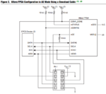
I have a JTAG head in the board, that is connected to the EPCS4. When I select JTAG in both the Programmer or the Signal Tap , I do not get device found. My only option is to select Active serial mode in the programmer, select the .pof and program the EPCS4.

Am I missing something?

Jose
 

That is because it's not a JTAG header.
Capture.PNG

You actually don't have JTAG connected to the FPGA unless there is another header somewhere or if you can access the breakout pattern for the FPGA and solder wires directly to the vias for the JTAG. I've done that before when I've been stuck working on a board that the board designer didn't add JTAG to the FPGA.

Regards
 
Separate active serial and JTAG programming headers for Altera FPGA have been superseeded about 10 years ago by the indirect JTAG programming method using a single JTAG header. It was introduced with Cyclone II FPGA family but can be even used with Cyclone I.

In the first years, many developers kept the old scheme with separate headers, also for Cyclone II. But I think, the advantages of the indirect JTAG programming method should become known in the meantime.
 
Hi,

Thanks for the discussion. The problem has been finally solved. A misunderstanding of the FPGA input (frequency selection signals) was in the end the root cause. A linear interpolator was interpolating always to zero . That combined with the ROM optimization described above was the cause. Now I have two beautiful LFM Chirp TTL waveforms out from my FPGA. I have to check the quality of the signals at the secondary of the transformer, but that s another issue.

Thanks again!

- - - Updated - - -

I presume you mean serial programmer connection. JTAG programming of serial flash (EPCSxx) goes through the FPGA and allows debugging as well.

I have not found the way of doing that with my PCB and Signal Tap. Can you point to a tutorial on how to use this debugging method with Signal Tap?
 

Status
Not open for further replies.

Part and Inventory Search

Welcome to EDABoard.com

Sponsor

Back
Top