Continue to Site

Welcome to EDAboard.com

Welcome to our site! EDAboard.com is an international Electronics Discussion Forum focused on EDA software, circuits, schematics, books, theory, papers, asic, pld, 8051, DSP, Network, RF, Analog Design, PCB, Service Manuals... and a whole lot more! To participate you need to register. Registration is free. Click here to register now.

Understanding an audio amplifier design

Status
Not open for further replies.

ArticCynda

Advanced Member level 1
Joined
May 8, 2013
Messages
439
Helped
82
Reputation
164
Reaction score
81
Trophy points
1,308
Activity points
4,238
Hi guys,

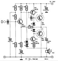
I've found an amplifier design online and built it, and it produces a nice sound quality from my laptop line out! I'm a newbie in transistor amplifiers however, and now I'm trying to understand how the circuit works. I've figured out the following so far:

- R1, R2 and C3 make a low pass RC filter to supply a clean base bias for T1
- R1, R2 and R3 divide the supply voltage to generate a bias voltage for T1
- R5 generates negative feedback to control the AC amplification of T1
- C1 couples the input signal into the preamp around T1
- T3, R7, R8, D1 and D2 make a current source of around 5.5 mA
- T4 and T5 are configured as push-pull power stage, and D3/D4 eliminates distortion due to T4/T5 Vbe offset
- C2 eliminates DC through the speaker
- C8 reduces ripple on the power supply

Now the questions:
- what is R6 for (I assume some sort of feedback)?
- what is C4 for?
- how does the second stage (T2) use the current source exactly?

Can someone hint on how to "calculate" this circuit? For example, how to find the DC emitter voltage of T1, or the base voltage of T4? An example would be awesome!

Thanks in advance!


Your attached schematic(?) does not work.
Thank you for your reaction!

It does work, I tested it with the line out of my laptop (~ 1Vpp) as audio input and a regulated DC supply of 15V. The only thing I changed are the power transistors T4 and T5 which I swapped for a TIP31 and TIP32 because I did not have the BD679 and BD680. But TIP31 and TIP32 are comparable, complementary NPN and PNP medium power transistors so that shouldn't make a difference (at least not for understanding the circuit). Or is that the wrong way to see it? I'm just starting with audio amplifiers, so please have some patience with me...
 

R6 is there to stabilize the output voltage between the output transistors. Ideally, it should be at half supply voltage so the output can 'swing' equally in both directions. If the DC at the output point increases, the feedback through R6 works to reduce it and bring it back to equilibrium.

C4 and R5 work together to control the amount of signal in the feedback loop. If you omitted them, the wanted output signal would be fed back through R6 and as described above, it would react so quickly that the audio you want would be completely compensated for, resulting in very little or no output. Obviously, you don't want to upset the DC part of the feedback so C4 is there to block DC conduction and allow the feedback to work properly. R5 is there to limit how much of the AC (audio) feedback is allowed into the loop. So the DC feedback goes straight through R6 and the AC feedback is dropped by the potential divider of R6 and R5. You should note that the value of C4 (it's reactance) increases as the frequency drops so it makes R5 appear to be a higher value and therefore allow more AC feedback. In fact the value of C4 decides the LF gain of the amplifier.

T2 is simply an amplifer stage, it's T4 that controls the current. It's a simple constant curent circuit, holding the base voltage constant with the two diodes makes the emitter voltage also stay constant so it will always pass ((2 * diode drops) - Vbe) / R7 Amps. As the Vbe and each diode will drop about the same voltage, it will set the current to approx 0.6/120 = 5mA.

Note that C2 should be rated at 25V if a 24V supply is used!

Brian.

edit: BD679 & BD680 are darlington transistors the TIP types are not. you probably need a lot more bias current to make the TIPs work properly.
 
T2 is simply an amplifer stage, it's T4 that controls
the current.
Brian,

I think this is a typo - T3 controls the current.

Also, what is the quiescent current of the output stage? With darlingtons and only two diodes it will be zero and I would expect a poor crossover response. A bit class C.

Keith
 
With a 15V supply and a 4 ohm speaker, the original circuit would have an output of about 11V p-p which is 3.9V RMS which is only 3.8W. The peak current in the output transistors is 1.38A.
The darlington output transistors have a current gain of typically 3000 so the drive current into them is fine. Since there is only two diodes to bias the output darlington transistors then they will produce crossover distortion.

TIP31 and TIP32 transistors have a current gain at 1.38A of typically 50 so the drive current must be 28mA peak which is not available from the circuit.
 
Keith, you are quite right. Finger trouble at my end - or old age - or, most likely a bit of both!

Brian.
 

Keith, you are quite right. Finger trouble at my end - or old age - or, most likely a bit of both!

Brian.
I know how you feel - it has been so cold recently I will have to start wearing gloves; my fingers have gone numb!

Keith
 

Thanks so much for all this info guys, this has been of great help to me!

Betwixt, your explanation of the function of R6 helped me to understand this circuit, and I now have a much better insight in the feedback mechanism. I wonder however, how the value of R6 can be calculated? Could you give an example of this, or refer to literature to help? I realize it's a voltage divider between R6/R5/C4, but I have no idea how to get the calculation "started" since neither the voltage on the emitter of T1 nor the currents, nor the DC voltage at the emitters of T4/T5 is known.

My attempt is the following: Vbe of T2 is 0.7V, so the collector current of T1 (assuming all transistors on) is 0.7/2k2. The base voltage of T1 is 15V * (270 / (270 + 150 + 33)), and its emitter voltage is 0.7V lower. This emitter voltage minus 1k5 * (0.7/2k2) is the emitter voltage of T4/T5. Is this correct?

When using darlingtons for T4 and T5, can I remove distortion by simply putting 2 more diodes in series with D3 and D4? Can I turn my TIP31 and TIP32 into darlingtons with another BC547 and BC557, or does this hurt my audio quality?

Audioguru, could you please explain how you get to the values of 11Vpp and 3.9V RMS? Can I make it work with just the TIP31 and TIP32 by simply increasing the bias current to 28mA by decreasing R7 to 0.65V/28mA?

Also, why is the current source set up around T3 connected to the speaker, and not grounded?

Thanks again for all your reactions guys!
 

Your consideration regarding DC feedback are basically correct. But you won't primarly vary R6 to adjust the DC bias point, better modify the base voltage divider.
You already considered R6 DC voltage drop, T2 base current can't be ignored neither for an exact calculation.

The R6/R5 divider sets the AC gain as required for the intended amplifier application.

The questionable output transistor bias has been mentioned by Keith. It seems to me that this is a rather sloppily designed circuit, I'm not sure if it's a good example to derive audio amplifier design methods.
 
I do not understand the purpose of the current source around T3 yet, why can't T3 and R7 be replaced by a single resistor to ground? What is the connection of this current source to the speaker for (e.g. why not referencing this to ground as well)?

You mentioned that it's a rather sloppily designed circuit. Could you perhaps suggest improvements to this circuit based on your expertise? I enjoy learning more about transistor amplifiers, and the best way to do that is listening to experts!
 

- Why is the T3 current source not connected to ground?
The structure is called bootstrap circuit, keeping the voltage across T3 almost constant. Usually the bootstrap circuit is combined with a single load resistor, providing constant bias current over output voltage and higher gain. The combination with a current source is a bit unusual, the only reason I can imagine is a slightly increased voltage swing.

- Why a current source instead of a simple load resistor? A resistor without bootstrap circuit would significantly reduce the output swing. A resistor with bootstrap circuit can work fairly, but the current source is keeping a constant bias current over supply voltage variations.
 
The current source made with T3 has a high impedance so that the open-loop gain of T2 is very high, much higher than if T3 is just a resistor. Then the distortion is very low when negative feedback is added.

T3 connects to the speaker instead of to ground for "bootstrapping" so that the negative-going signal from the speaker drives T3 and the base of T5 below ground for a high output swing amplitude. Bootstrapping also increases the impedance of the T3 current sink for a high open-loop voltage gain for T2.

Since the output transistors are darlington types that have two base-emitter junctions in series for each darlington then 4 series diodes should be used to bias them instead of only 2 diodes. Actually a transistor should be used instead of diodes to provide an adjustable voltage to bias the output transistors.

Most half-decent audio amplifier circuits and ICs use a differential amplifier at the input. Also they have current-limiting circuits to protect against a shorted output.
 
Last edited:
Now the questions:
- what is R6 for (I assume some sort of feedback)?
- what is C4 for?
- how does the second stage (T2) use the current source exactly?

... how to "calculate" this circuit? For example, how to find the DC emitter voltage of T1, or the base voltage of T4? An example would be awesome!

See the current & voltage notations at your schematic below. The calculated values refer to an operating voltage of 24V and a loudspeaker resistance of 16Ω. For simplicity I assume all Vbe voltages = 0.7V .
audio-amp.gif
Here the calculations:

1. Base voltage of T1: VBT1 = (R3/(R1+R2+R3))*24V = 14.3V
2. VET1 = VBT1 - VBET1 = 13.6V
3. Collector/Emitter current of T1: IT1 ≈≧ VBET2/R4 = 0.32mA
4. VET4 & T5 = VBT1 - IT1*R6 = 13.1V
5. IT3 & T2 = 0.7V/120Ω = 5.8mA
6. VLS = (IR8+IT3 & T2)*RLS ≈ 0.3V (estimated)
7. VBT3 = VLS + 2*0.7V = 1.7V
8. IR8,D1,D2 = (24V - VBT3)/R8 = 12.4mA
9. The LS output at the lower node of R7 bootstraps (= nearly 100% of positive feedback) the T3-T2 stage in order to provide larger output swing
10. R6/R5 defines the ac gain of the amplifier
11. C4 enables DC gain = 1 (full negative DC feedback from output to "input": T1 emitter ac voltage ≈ T1 basis ac voltage).
12. 1/(2πR5C4) creates one of the lower -3dB frequency limits (48Hz) of the amplifier gain. 1/(2πRLS*C2) establishes one more lower frequency limit (4.5Hz)
 
Thanks so much for the assistance guys, and most notably erikl for doing the effort of providing an actual calculation example!

Audioguru, doesn't the series capacitor C2 automatically protect the output against a short circuit? I would assume that since T3 is a fixed current source, it cannot be shorted. Or is that the wrong way of thinking?

FvM, does this imply that, if I would replace the current source around T3 with a simple resistor, that my output volume increases with supply voltage? I'm at the moment trying to figure out how to calculate the AC amplification of the circuit, so my apologies if this sounds as a stupid question at this point.
 

Audioguru, doesn't the series capacitor C2 automatically protect the output against a short circuit? I would assume that since T3 is a fixed current source, it cannot be shorted.
Simply calculate the reactance (AC resistance) of C2 at an audio frequency such as 1kHz. It is only 0.07 ohms and is less at higher frequencies. So when the output is shorted then the output transistors T3 and T4 will produce an extremely high current through C2 to the short when the amplifier is playing. T3 is the load for T2, it does not drive C2.

if I would replace the current source around T3 with a simple resistor, that my output volume increases with supply voltage? I'm at the moment trying to figure out how to calculate the AC amplification of the circuit.
Without negative feedback the voltage gain of T1 plus T2 is very high. The current sink made with T3 has a very high impedance which makes the gain of T2 very high. R6 and R5 form the negative feedback then the voltage gain of the entire circuit is R6/R5= 10.
 
Last edited:

Status
Not open for further replies.

Similar threads

Part and Inventory Search

Welcome to EDABoard.com

Sponsor

Back
Top