qwertyx
Newbie
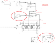
I am studying the schematics of an analog isolator with variable gain (SIM 984 from SRS0, the isolator is bipolar and can handle positive and negative voltages).
In the isolation part of the schematics (see picture attached), the author uses two voltage references circled in red.
Having read the manual of the analog optocoupler used here (HCNR200, see p.19 4th paragraph - circuit 15a- of the HCNR manual (https://docs.broadcom.com/doc/HCNR200-HCNR201-High-Linearity-Analog-Optocouplers-DS)) I think that these voltage references are used as current sources, the first one on the top left offsets the current so that it appears unipolar to the photodiode, and the second one offsets it again the other way so that the signal recovers its original polarity.
The thing is, on the input side for example, the voltage Vin can reach up to +/-1000V according to my understanding of the device and given the input resistor the current can reach +/-10mA. So if say the current reaches -10 mA the voltage reference must source 10 mA for the current to stay positive, this is because I am assuming the op amp to be ideal and that no current flows into the inputs. But at best the current sourced by the voltage reference is 5/38300<<10 mA. It feels like the voltage source is pointless. So how does this work?
The full schematics can be found on (https://xdevs.com/doc/Stanford_Research_Systems/SIM900/sim984_sch.pdf)