Welcome to our site! EDAboard.com is an international Electronics Discussion Forum focused on EDA software, circuits, schematics, books, theory, papers, asic, pld, 8051, DSP, Network, RF, Analog Design, PCB, Service Manuals... and a whole lot more! To participate you need to register. Registration is free. Click here to register now.
You should consider the possibilty, that the room occupied by a component (the so-called courtyard) is larger than the rectangle enclosing the pads. In my opion, the datasheet is soooo obvious...
Correct. 10.4mm x 10.4mm is the dimension of the coil. The two pads shown at 11 x 3.6 are where you put the pads for the part to solder to. Normally you would create a footprint with the pads as shown in the drawing and then add a no-go area and silk screen to show the overall outline of the part.
Keith.
---------- Post added at 10:04 ---------- Previous post was at 09:54 ----------
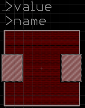
Here is what it might look like
You can see the pads. The rectangular area is a "keepout" area. This inductor is slightly different to yours - it is a shielded rectangle rather than open.
This site uses cookies to help personalise content, tailor your experience and to keep you logged in if you register.
By continuing to use this site, you are consenting to our use of cookies.