Welcome to our site! EDAboard.com is an international Electronics Discussion Forum focused on EDA software, circuits, schematics, books, theory, papers, asic, pld, 8051, DSP, Network, RF, Analog Design, PCB, Service Manuals... and a whole lot more! To participate you need to register. Registration is free. Click here to register now.
Hi
ohhh, No
PMOS bulk is connected to source in that schematic.
but P-N junction of bulk-drain cab be forward bias in this situation.
so, for correct operation of switch in this example bulk of NMOS must be connected to Vdd.
for NMOS it depends technology that you are using. if you have twin-well there is no problem to connect NMOS bulk to anywhere but if you have just N-well you mist connect all NMOS Bulks to the lowest voltage in your circuit.
regards
Thanks hr_rezaee,
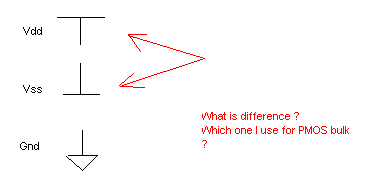
I understood that NMOS Bulk is connected to the ground and PMOS Bulk to the source. I'm confused because I have 3 components in my analog design envirement library which are the following:
Hi
it is just a name.
you must connect it to highest voltage that can be across PMOSs.
if this voltage is Vss, you must connect it to Vss.
but Vss is usually below zero potential.
regards
This site uses cookies to help personalise content, tailor your experience and to keep you logged in if you register.
By continuing to use this site, you are consenting to our use of cookies.