Continue to Site

Welcome to EDAboard.com

Welcome to our site! EDAboard.com is an international Electronics Discussion Forum focused on EDA software, circuits, schematics, books, theory, papers, asic, pld, 8051, DSP, Network, RF, Analog Design, PCB, Service Manuals... and a whole lot more! To participate you need to register. Registration is free. Click here to register now.

Transmission Gate Output strange behaviour

Status
Not open for further replies.

brakchus

Newbie level 4
Joined
May 21, 2009
Messages
7
Helped
1
Reputation
2
Reaction score
0
Trophy points
1,281
Activity points
1,357
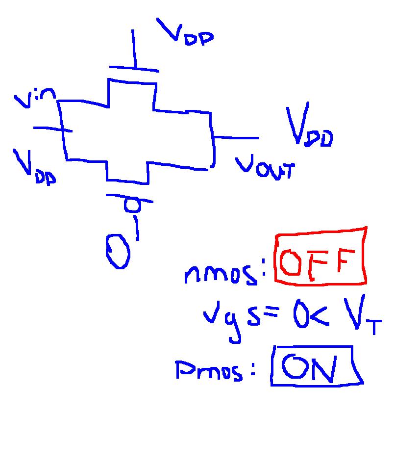
Hi, I have TG design as in the picture below:

**broken link removed**

while the enable and ~enable signals (at transistors gates) was from Virtuoso Analog Design Environment as stimuli signals, the output was just as I expected. After I added an inverter the output change. The result is in the picture below:

**broken link removed**

Can anybody give me a clue, why the output isn't always at gnd level? And sometimes even over vdd?
 

Probably time-delayed charge injection difference (before, presumably there was no delay between enable & ~enable). Try and add a (high) resistive load at the output (≈ 1MOhm)!
 

The output is not always at ground because your input is moving. The transmission gate's output is always trying to follow the input voltage.

Vin =0.5 V, given long enough time, Vout = 0.5. This is why its not 0.

It goes over Vdd because of the charge injection mismatch when you are turning off the tranmission gate.

charge injection has 2 components. The physical overlap/fringe capacitance between the gate and the drain/source. This component of the charge injection will be relatively closely matched.

charge injection thats not matched comes from the charge stored in the channel.

consider the case with Vout is close to Vdd. The nmos is turned off here--> no electrons in the channel of the nmos. In the pmos, there is a layer of inversion charge at the surface. These holes carry positive Charge. When turn off this device, the holes have to go some where. approx 1/2 of them go to the source, 1/2 go to the drain. the holes that go to the output increases the voltage on the output node as shown in the simulation.

Added after 6 minutes:

also you can see when Vout is close to 0 .

here, the pmos is turned off (no holes in the channel in the pmos) but the nmos is turned on, with lots of electrons in the channel. When this device is switched off, the electrons splits. the electrons that make it to the output node causes the output node's voltage to go below gnd.
 

eecs4ever said:
... the pmos is turned off (no holes in the channel in the pmos) but the nmos is turned on ...
In a TG, both the pmos and the nmos are on (or off) nearly simultaneously!

eecs4ever said:
When this device is switched off, the electrons splits. the electrons that make it to the output node causes the output node's voltage to go below gnd.
When this device is switched off, the nmos is switched off one inverter delay earlier than the pmos, hence the pmos cannot have been turned off before (s. above), it will be turned off one inverter delay later than the nmos, then delivering its positive charge likewise to the output.
The voltage shift may result from a difference between the 2 charges, as indicated in my former posting - and should vanish with a resistive load.
 

erikl said:
In a TG, both the pmos and the nmos are on (or off) nearly simultaneously!


No, the transistors in the TG are on/off depending on the voltage being passed through.

consider Vout = Vdd
EN = Vdd

Vgs of the nmos switch is 0

nmos is off. pmos is on.
 

eecs4ever said:
No, the transistors in the TG are on/off depending on the voltage being passed through.
No, sorry, your understanding of a TG is not correct: A TG shall either transmit or not transmit from input to output (or vice versa), depending on its "on" or "off" state, and independent on the voltage being passed through. I.e. both the nmos and the pmos are either "on" or "off" at the same time, as stated previously. S. the schematic in the original posting!

eecs4ever said:
consider Vout = Vdd EN = Vdd
Vgs of the nmos switch is 0
nmos is off. pmos is on.
No; nmos is off when EN=0, then pmos is off, too: via the inverter, its gate receives a logical "1" (vdd), which means Vgs of the pmos is 0, too, hence it is also off. Just study the schematic above thoroughly!


Erikl, your understanding of basic transistor properties is incorrect. the MOSFET is a 4 terminal device. Whether is ON or OFF doesnt depend only on the gate voltage. It also depends on the source, drain, and body voltage.

There are clearly many cases in the TG circuit where only 1 of the nmos or pmos device is on while the other is off.
 

Still, you changed only the phasing and you got a different
result, that is where you should look. Unless you did other
things you haven't noticed, or explained.

There are plenty of analog switches where you conduct
through both FETs at once. The first to turn off, has its Qgd
charge returned to the source by the switch that is still on.
The last to turn off, has nowhere for its Qgd to go because
the other is off already. Except to sit there at the now-high-
impedance output. This is how you get an asymmetric
(hence not-GND) charge pedestal.

Try sliding the phase of NMOS relative to PMOS gate, and
see what happens.
 

After some thinking, I've done some more simulations to better understand what exactly is going on. I wanted to be sure that strange behave is done by adding an inverter.
1st simulation: TG without inverter, but with R=1MOhms at OUT. Results:
**broken link removed**
EN and ~EN signals are stimuli pulse signals. When ~EN is equal to 1 both transistors are in cutoff region, but there is some charge - probably capacity I think. We can see that creating path to gnd trough resistor is good way to discharge this accumulated energy.

2nd simulation: TG with inverter, without R. Results:
**broken link removed**
EN is stimuli pulse, ~EN is from inverter. When ~EN is equal to 1 both transistors are in cutoff region, but without R the charge accumulated in parasitic capacity have no way to go.

3rd simulation: TG with inverter, but with R=1MOhms at OUT. Results:
**broken link removed**
EN is stimuli pulse, ~EN is from inverter. When ~EN is equal to 1 both transistors are in cutoff region. The result is very similar to 1st simulation.

After all, the inverter isn't so bad;) Even without R, current isn't passing through TG, so TG isn't draining current when EN=0 and thats what I wanted to achieve.

Thanks everybody for discussion and help. I hope screenshoots will help other people to better understand TGs.
 

    V

    Points: 2
    Helpful Answer Positive Rating
Status
Not open for further replies.

Part and Inventory Search

Welcome to EDABoard.com

Sponsor

Back
Top