bagan
Newbie
hi,
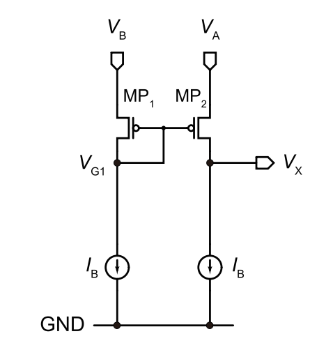
If VB is fixed voltage, and VA > VB, output Vx will change from low to high.
The input offset error primary determined by mismatch of IB for both branch and also the size of transistor MP1 & MP2. IB can be implemented using cascode current mirror to increase its impedance and the size MP1 & MP2 can be made large to reduce VGS mismatch.
My question is how to check the input offset error for this kind of amplifier in simulation?
Thank you very if someone can clear my doubt here. .