Continue to Site

Welcome to EDAboard.com

Welcome to our site! EDAboard.com is an international Electronics Discussion Forum focused on EDA software, circuits, schematics, books, theory, papers, asic, pld, 8051, DSP, Network, RF, Analog Design, PCB, Service Manuals... and a whole lot more! To participate you need to register. Registration is free. Click here to register now.

Transistor Driver Circuit Question

Status
Not open for further replies.

themaccabee

Full Member level 4
Joined
Apr 1, 2007
Messages
201
Helped
6
Reputation
12
Reaction score
6
Trophy points
1,298
Activity points
3,003
Hi ,
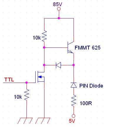
I need to design a driver circuit to switch a PIN diode ON and OFF,
When switched ON the forward current should be in the range 50-100mA, im considering the following circuit..(the transistor Vbe max is only 5V)
Does it have any problems?
Thanks & regards
0_1306039924.jpg
 

You can place the diode in the drain of the mosfet and through a resistor to the 85v power supply so why do you use the transistor and the extra components?
You mosfet can obviously work with 85v so 100mA shouldn't be a problemand if it is use a different mosfer.
You will have a few watts on the resistor you will use because of the voltage drop (about 84v*0.1A=8.5W)

Alex
 

Your PIN diode has two operating states:
1. open, with a current you say 100 mA
2. closed, no current but ~90 volts in reverse.

Your circuit can work but as others wrote, some devices will have to be cooled.
If you do not really need full 85-90V in reverse, you can use a "power optocoupler" which allows current up to 2 A (PVG612). You never specified switching speed; for < 1 us, your circuit can be better.
Sometimes it is easier to install the PIN diode with one end grounded. Then using the optocoupler can be easier to use.
 

You will have a few watts on the resistor you will use because of the voltage drop (about 84v*0.1A=8.5W)
Sorry i couldnt understand that can u please explain..Is it the 10k base resistor or the 100R resistor that you were mentioning..

I was thinking like when the MOSFET is OFF transistor is ON PIN diode being reverse biased approximately no current flow through the 100R ..
Then when the MOSFET is ON transistor base is at 0V and 50mA(5V/100R) current flow through the 100R resistor--> PIN diode (Forward biased)-->diode-->MOSFET-->GND.

Please correct me if im wrong..
Your circuit can work but as others wrote, some devices will have to be cooled.
So can you explain me the high power dissipation like 8.5W( for 100mA or if 50mA then 4.2W) arises..& which devices exactly has to be cooled?

High switching speed ( comparable to 1uS) is not needed 1 -5ms will suffice.
Thanks for any help.
Regards
 
Last edited:

When the NMOS is cutoff, a negligible current flows in the 10K resistor, so no heating.

When the NMOS is on (0V), the power dissipation in the 10K is 85*85/10K = 722mW (2W resistor works).

Kerim

Added:
Also when the NMOS is on (0V), the power dissipation in the 100 ohms is (5-1.4)^2/0.1K = 130mW (400mW resistor works).
Note: This analysis is for DC only, the actual dissipations will likely be a bit higher.
 
Last edited:
Sorry i couldnt understand that can u please explain..Is it the 10k base resistor or the 100R resistor that you were mentioning..

I was thinking like when the MOSFET is OFF transistor is ON PIN diode being reverse biased approximately no current flow through the 100R ..
Then when the MOSFET is ON transistor base is at 0V and 50mA(5V/100R) current flow through the 100R resistor--> PIN diode (Forward biased)-->diode-->MOSFET-->GND.

I didn't notice the 5v supply, so the operation will be as you have described but I don't understand why do you have that 85v connected.
Do you want to test the reverse polarity of the diode in a high voltage?

Alex
 

Under 100 mA through the PIN diode, the 100 Ohm resistor will dissipate ~ one watt but the NPN transistor will have to dissipate more.
The full voltage from +85V to -5V is 90v, across the 100 Ohm resistor , 10 V; then I estimate almost 80V should be across the NPN transistor, close to 8W will have to be dissipated.
The requester never mentioned the PIN diode type; from the 100 mA open and 90V closed I guess it is used in a high-power switch application, the high power referred to the RF signal to be switched. For a RF power under one watt, the PIN diode current and voltage may be smaller than 0.1 A and 90 V.

Sorry but how did you get from the circuit... the 100mA? When the pin is forward biased its current is approximately (5V-0.7-0.7)/100 ==> 36mA.
And also based on the circuit, how the current from the 85V supply can go through the 100R resistor? The pin diode in this case is reversed biased hence if (85-5)=80V is under its breakdown voltage, its current is very small (negligible),
 
Last edited:

Under 100 mA through the PIN diode, the 100 Ohm resistor will dissipate ~ one watt but the NPN transistor will have to dissipate more.
The full voltage from +85V to -5V is 90v, across the 100 Ohm resistor , 10 V; then I estimate almost 80V should be across the NPN transistor, close to 8W will have to be dissipated.
The requester never mentioned the PIN diode type; from the 100 mA open and 90V closed I guess it is used in a high-power switch application, the high power referred to the RF signal to be switched. For a RF power under one watt, the PIN diode current and voltage may be smaller than 0.1 A and 90 V.

the 5v voltage is positive not negative.
When the transistor is on then the diode under test will be reverse polarized so there will be no current through the transistor or the diode.
The 50-100mA will flow only through the mosfet (when it is turned on) and the two diodes and the 100 ohm resistor, there will also be a lower current through the 10K resistor.

Alex
 

I think the PIN diode is painted reversed in the circuit.
Without a TTL HI input, the NPN transistor is open and then 100 mA can flow through the PIN diode. With TTL HI, the NPN transistor closes and there will be no current through it.
 

No, the pin diode direction is correct.
When the mosfet has a LOW in the gate it is off so the 10k works a as a pullup and turns the transistor on to apply reverse bias to the diode under test.
When the gate is high then the transistor base has a low voltage that turns it off, in that case the diode under test has forward bias and the current flows between gnd-mosfet-diode-pindiode-resistor-5v

Alex

Well explained
 
Status
Not open for further replies.

Part and Inventory Search

Welcome to EDABoard.com

Sponsor

Back
Top