Continue to Site

Welcome to EDAboard.com

Welcome to our site! EDAboard.com is an international Electronics Discussion Forum focused on EDA software, circuits, schematics, books, theory, papers, asic, pld, 8051, DSP, Network, RF, Analog Design, PCB, Service Manuals... and a whole lot more! To participate you need to register. Registration is free. Click here to register now.

I have a question about the conditions under which the transistor dies.

RFchild

Newbie level 4
Joined
May 24, 2024
Messages
7
Helped
0
Reputation
0
Reaction score
0
Trophy points
1
Activity points
57
Hi, I’m a student.
I designed LNA using renesas’s jfet NE3511S02.
But I have some problem.
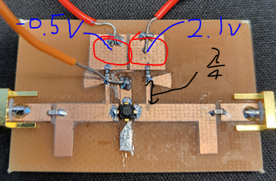
I designed the rf choke using 4 lambda, but does the length of the red hit part in the picture matter?
1716555412805.png
And I mesured the circuit using network analyzer, then the transistor is dead.
Did I accidentally design the rf choke and get a oscillation and die?
Or did TR die when soldering?
On ADS simulation, stability mu is more than 1. But stability factor k is less than 1.
Is it the matter?
 
Microstrip Lines and RF Connections seem to me not normal.
Transistor can be blown by anyhow such as ESD, Oscillations, unappropriated biasing.
But first of all, the layout does not look promising. There are errors.
 
Microstrip Lines and RF Connections seem to me not normal.
Transistor can be blown by anyhow such as ESD, Oscillations, unappropriated biasing.
But first of all, the layout does not look promising. There are errors.
sorry, I don't have enough knowledge about rf. Can you tell me some errors?
 
Sorry but the results are NOT satisfying. You make Design Mistakes. Review your Design and Re-Iterate.
Also..
You're using a s-parameter defined transistor model and DC supply has no importance/role at all at this level. You can replace the DC supplies with short-circuited.
You cannot see bias currents and voltages because the transistor has been modeled by small signal s-parameters. I predict a much better result from this transistor.
Layout must carefully be designed and Coupling, De-Coupling, Connectors and other stuffs have to be very carefully and attentively designed and placed because you're working around 10GHz and small things impact much the circuit's performance.
Thank you! I will re-design the circuit.
And I have one more question.
The stability factor 'k' is less than 1, but 'mu' is more than 1.
This situation the circuit is stability? or unstability?
 
Thank you! I will re-design the circuit.
And I have one more question.
The stability factor 'k' is less than 1, but 'mu' is more than 1.
This situation the circuit is stability? or unstability
For more information.
 
I don't know what substrate you used. For example, 0.3 mm Rogers Duroid RT5880 with Glass or Ceramic and PTFE mixed or just ceramic is far more expensive and will be much thinner but more stable.

It could also be laid out in a small rectangular area for your LNA with a connector for external DC bias or onboard with a regulator. This improves rigidity and a lower noise figure (0.3 dB). You can then mount the RF connectors to the material and include a 1/4" FR4 board for mechanical stability and a power plane if needed, in future.

This LNA FET has a max. current of only IDSS and is very low power and is very ESD sensitive. Consider large pads also as a patch antenna unless well connected with many u-vias to some large ground plane.

The datasheet uses a Rogers material equal to 0.254 mm thick to make a coplanar ground wave (=source).

You appear to be using something that computes to 1.6 mm thick from the trace widths. This thickness naturally increases dissipation losses somewhat.

Although the device is only rated 5for 1/6 W, you need many microvias commonly called "thermal vias" to reduce the interlayer inductance.

Can you verify your thickness, ground and DC decoupling schematic showing the parasitic inductance and s-parms for the decoupling cap.
You did not show a logic diagram, which is useful to include these assumptions and details. You may want to use a coplanar wave design for slightly better performance with topside emissions. This also affects trace width. Generally trace w/t width to thickness is about 2:1 with log variations due to relative permeability Er. The inductance of a square is constant for all area sizes but then increases by length.

If seems you chose Vdd=2.1V, Vgs= -0.5 V which seems to be the most non-linear bias instead of -0.2V for some reason.

1716663739217.png


A preferred layout might look like this;
1716664321861.png


The wide tolerance on Vgs requires an active Vgs bias circuit.
1716665698494.png

Here are some library search results I made for you.

Note the company mergers:

California Eastern Laberatories + Renesas + NEC = Renesas
 

Attachments

  • 1716663628652.png
    1716663628652.png
    11.8 KB · Views: 22
Last edited:
How do you know the transistor is dead?
In my opinion (looking to the designed circuit) the transistor is alive, but placed in your poor made circuit is not amplifying anything at Ku band.
On your PCB you need a top ground also, ideally connected through vias to the bottom ground, as seen in #15.
I am afraid that your fabricated PCB is FR4, which is totally inappropriate at 10GHz.
 
I've seen many times this kind of discussions, about FR4 behavior at frequencies greater than 10GHz.
Unfortunately not all the PCB performances are related to loss, even if losses are the most important characteristics.
Think that you are optimizing the noise figure of an LNA (just with fractions of dB), and suddenly you increase with few dB's the system noise figure, only because you are using a lossy substrate.
The same is when designing a power amplifier, when loose many watts just because of using a lossy substrate.
 
Anyone using a Fire Retardant level 4 material (FR4) for frequencies above 900 MHz in critical applications has a lot to learn about dielectric losses, dispersion effects from microstrip, surface roughness, skin effects on impedance, broadband vs narrow band and DFT with suitable connectors.

Here, 0.2 dB NF LNA @ 10GHz is a very critical spec.

Your results will depend on the quality of your measurements, choice of materials, and logical design with parasitic included in the logic diagram. I suggest that both a symbolic (logic) diagram and physical diagram with impedance values, and tolerances, considering that Dk and Df loss factors both change with frequency. All discrete parts must also state loss ESR = DCR and SRF or ESL.

It is normal to make mistakes on your first few attempts. This is how you learn.


One catalogue of RF substrates.
 
where are your capacitors on the bias lines?

yes, at ONE FREQUENCY that radial open circuited stub will create an RF short circuit. but what about frequencies above where it is one quarter wavelenght long. Or what about lower freqencies like 100 MHz, where that transistor has gobs of gain.

you need to add 1000 pf capacitors to ground right after where the two radial stubs meet the thin bias line. ALso, it is traditional to also have a 1 uF to 4.7 uF cap on the drain bias line too.
 

LaTeX Commands Quick-Menu:

Part and Inventory Search

Welcome to EDABoard.com

Sponsor

Back
Top