Continue to Site

Welcome to EDAboard.com

Welcome to our site! EDAboard.com is an international Electronics Discussion Forum focused on EDA software, circuits, schematics, books, theory, papers, asic, pld, 8051, DSP, Network, RF, Analog Design, PCB, Service Manuals... and a whole lot more! To participate you need to register. Registration is free. Click here to register now.

Transistor base at high voltage

Status
Not open for further replies.

tiwari.sachin

Full Member level 6
Joined
Aug 1, 2009
Messages
341
Helped
3
Reputation
6
Reaction score
3
Trophy points
1,298
Location
India
Activity points
4,449
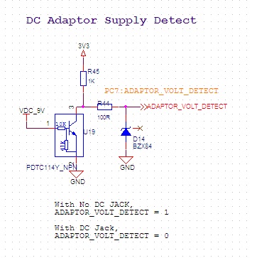
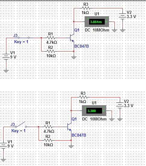
Can I use a npn/pnp transistor and drive the base with 9V (I know its current that drives it) but base will have 9V

I need to have a output @ 3.3V. I will connect collector to 3.3V for npn and Emitter to 3V3 in case of pnp.

I am using BC847B or BC856

Is something like this reliable??? or for that matter can i even use something like this
 

I could be wrong, but for a PNP it may be risky to apply a bias voltage which has greater positive amplitude than the supply. It is because of a characteristic similar to zener effect in the pn junction. This might result in unwanted current flow from your 9V signal into the 3.3V power source.

(You'll sometimes see an unconventional 'gimmicky' circuit which makes use of this effect.)

I could be wrong because the effect might be confined to NPN type.
 

You make no sense.
If the collector of an NPN transistor is +3.3V then the base voltage can go no higher than about 0.7V higher to +4V because the base-collector diode conducts.
If the emitter of a PNP transistor is +3.3V then the base should not go up to +9V because the maximum allowed reverse emitter-base voltage for a BC856 is only 5V. A higher voltage might cause avalanche breakdown that causes conduction and damage.
 

Well, with a stiff enough power supply he -could- impose
9V. At least until the bond wires fuse.

Each pin has a voltage and a current upper bound and
negative lower bound. It helps nothing to consider only
one of them and ignore the other. Often enough the
first destructive limit attends the one you chose to neglect.
 

How about using a voltage divider and then connecting that to the base.

I want to have a circuit that detects 9V adaptor supply and is input to the MCU which works on 3.3V

I could only use a voltage divider but I am not sure how to take care during hot plug in of DC adaptor

Because DC adaptor voltages can vary (say 7.5 to 12V approx), voltage divider will have effect and MCU pin can damage
 

Hi,

Can I use a npn/pnp transistor and drive the base with 9V
The absolute voltage is not of interest, only referenced to emitter (sometimes collector, too).
The NXP_PHILIPS BC847 datasheet says max voltage Veb = 6V (mind the direction: emitter to base)
And the typical Vbe = 0.66V. It depends on base current. You need a base current limiting resistor.

****
About your circuit...
You must not feed the 9V to a 3.3V MCU. How do you step down?
Maybe a simple diode does the job..

Klaus
 

I was thinking of using the same as explained above but that seems to be dumb idea

How about using a voltage divider and then feeding it to transistor or perhaps use a cheap LDO or a zener regulator
 

I simulated the initial transistor circuit that I was referring to using a transistor and it seems to be working


I am using multisim.
 

Hi,

You simulate a totally different circuit than you described in your fist post:
but base will have 9V
--> in you simulation it never is 9V!
I will connect collector to 3.3V for npn
--> in simulation a pullup resistor is connected to 3V3!
I need to have a output @ 3.3V.
--> my assumption on this was, that you want the 3V3 for supplying your circuit, instead of a 3V3 logic signal.
Indeed the transistor output pulls to 0V only. The 3V3 come from an independent supply with a series pullup resistor.

*****
In future please describe it more precisely, or attach a photo of a simple draft.
Thanks

*****
Are there still any concerns about your circuit?

Klaus
 

@KlausST.... I am soo sorry if i was not able to explain it clearly. I too initially thought I will simulate and send it but somehow missed it... My sincere apologies for making it confusing.

I will surely attach the schematic in future. I agree that it will make things clear.

So the initial circuit is good enough then :)
 

The 10K Resistor to ground in your Circuit is NOT in the correct place.
If you want to use it, It should actually connect to the Base of the Transistor.
 

A transistor switch is often defined with a current gain of only 10:1 ratio in daasheets for Ic:Ib ratio. THis is common for most transistors except the very best which are 50:1 or 10% of the hfe.

TO minimize input current and turn off speed the pull down input and pull up output is a factor with diode capacitance only when high speed is a concern.

Thus the R values are always determined by the necessary load current and capacitance.

The output equivalent ON resistance can be defined by the input base current from this saturated Ic:Ib ratio as a linear resistance in effect, Vc/Ic= Rce which must be much lower than the pull up resistance to be saturated low Vce. THis can be estimated easily to be << 10% of load R pullup to get <<10% of 3.3V for example and satisfy logic low conditions.

AS chemelec suggests the turn off base resistor is normally across Vbe to reduce input current loading and raise input impedance.
 

I did check this and its working fine. Below is the sch


Now if I plugin/plug out DC (9V), Will that hotplug effect the performance.

I am using R44 and D14 for protection.

Adaptor is a SMPS (9V/3.5 Amps).
 

If you want the transistor to simply turn on and make the output a low voltage when 9V input is present then the 100 ohm resistor R44 and the zener diode D14 with no voltage rating are not needed.
When there is no 9V then the transistor will simply turn off or stay turned off then R45 will make the output high if it feeds a high resistance.
The 9V is an input and can be applied or disconnected at any time with no problems.
The transistor is not even needed and can be replaced by a voltage divider made with two resistors (then the logic will be inverted).
 

I could have used voltage divider but 9V (comes from adaptor) can vary... Say between 9-10V... thats why prefer a transistor.

My concern really is... will surge have effect... I am not sure if i can even refer it as surge (plug unplug of DC Jack)... I want a low on MCU when DC Jack is plugged so that the MCU knows from where it is getting its power.... From DC jack or battery.
 

Hi,

I can't find the pdf, maybe it was a schematic in a web page, sorry, think it discussed the use of TVSs. An Arduino or something like that had a curious schematic (by an engineering company, it was a real device) where the input came from a DC adapter or PC USB, from memory if I recollect well, and the input went to a 5V regulator and a 3.3V regulator... Sorry I can't find it, it sounds useful for what you are doing. Maybe looking at schematics which include the inputs to those devices will give you ideas you can work with.

- - - Updated - - -

My concern really is... will surge have effect... I am not sure if i can even refer it as surge (plug unplug of DC Jack)..

...Only for this concern, the Vishay pdf on page 6 onwards, and page 26 or so have block layouts to deal with this issue, hope it's of some use.

View attachment Diodes and MOVs uses 49337 Vishay.pdf
 

Overall your design is poorly defined.

What are all input V ranges?
Is there undervoltage protection (UVP)?
Will transfer voltage be stable during line transient?
What current max do you want for voltage sense signal and how does that affect battery life?
What surge current do you expect?
i.e. What is the ESR of hidden supply caps and what is contact surge current rating? ( Joule rating of discharge/charge affects contact life. of jack )

There will be contact bounce on jack, so will you filter signal in hardware or software?

Always start a design question with a list of assumptions or a spec.
 

Overall your design is poorly defined.

What are all input V ranges?
Is there undervoltage protection (UVP)?
Will transfer voltage be stable during line transient?
What current max do you want for voltage sense signal and how does that affect battery life?
What surge current do you expect?
i.e. What is the ESR of hidden supply caps and what is contact surge current rating? ( Joule rating of discharge/charge affects contact life. of jack )

There will be contact bounce on jack, so will you filter signal in hardware or software?
/QUOTE]


What are all input V ranges? : 8.5 to 10V
Is there undervoltage protection (UVP)? Yes there is
Will transfer voltage be stable during line transient? Expect it to

What current max do you want for voltage sense signal and how does that affect battery life?

The voltage detect signal drives the MCU pin and hence about 20 odd mA. When the DC jack input is detected, the power from the battery is cutoff and all the current is drawn from DC Jack

What surge current do you expect?

i.e. What is the ESR of hidden supply caps and what is contact surge current rating? ( Joule rating of discharge/charge affects contact life. of jack ).

I am really not sure about this part. Need to check but I am not sure if I will get proper details. Let me try.

Contact Bounce on Jack: I would prefer to handle that on hardware but not sure how to do it.

The DC jack voltage drives DC to DC, LDOs and that inturn powers the remaining circuit
 

Taking a cue from post #14, which points out that "the transistor is not even needed"...

If you have the right zener diode, that will prevent incoming voltage from rising above 3.3 V.
Or two red led's can stand in.

7606484900_1448348458.png
 

If you have the right zener diode, that will prevent incoming voltage from rising above 3.3 V.


7606484900_1448348458.png


I did think of the concept you said but somehow decided to use transistor. I dint want the MCU to blow in case the zener goes bad

What about the scnerio when 9V is not connected. I need a low at MCU pin. Shouldnt I be using a 100nF cap at output so that it is low when no load in connected.
 

Status
Not open for further replies.

Similar threads

Part and Inventory Search

Welcome to EDABoard.com

Sponsor

Back
Top