Winny_Puuh
Junior Member level 1
Hey guys,
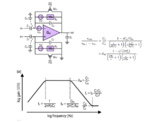
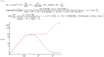
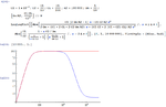
I've got a few questions concerning the following schematic.
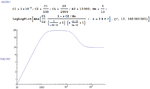
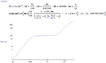
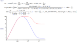
1. Most importantly... how can I calculate that transfer function? I'll just never get the same result as they do in the paper...
2. Does anyone know what kind of feedback that is? What does it do?
3. Why is the formula for the high cutoff frequency fH=gm/(2PiAmCL)?
Hope someone can help
Winny
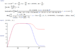
I've got a few questions concerning the following schematic.
1. Most importantly... how can I calculate that transfer function? I'll just never get the same result as they do in the paper...
2. Does anyone know what kind of feedback that is? What does it do?
3. Why is the formula for the high cutoff frequency fH=gm/(2PiAmCL)?
Hope someone can help
Winny