Continue to Site

Welcome to EDAboard.com

Welcome to our site! EDAboard.com is an international Electronics Discussion Forum focused on EDA software, circuits, schematics, books, theory, papers, asic, pld, 8051, DSP, Network, RF, Analog Design, PCB, Service Manuals... and a whole lot more! To participate you need to register. Registration is free. Click here to register now.

Transfer function & high cutoff frequency

Status
Not open for further replies.

Winny_Puuh

Junior Member level 1
Joined
May 1, 2013
Messages
17
Helped
0
Reputation
0
Reaction score
0
Trophy points
1,281
Visit site
Activity points
1,461
Hey guys,
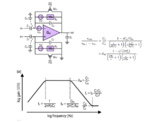
I've got a few questions concerning the following schematic.
1. Most importantly... how can I calculate that transfer function? I'll just never get the same result as they do in the paper...
2. Does anyone know what kind of feedback that is? What does it do?
3. Why is the formula for the high cutoff frequency fH=gm/(2PiAmCL)?
Hope someone can help
Winny
 

Attachments

  • frage.PNG
    frage.PNG
    54.1 KB · Views: 202

I notice they say the gain at very high frequency is C2/CL. This means that if CL is zero, the gain is infinite. Does this make sense?

Where did you get this schematic? Have you tried simulating it?
 

The equatitions apparently involve some simplifications respectively inaccuracies. CL stands for the total load capcitance, which would include C2.

Nevertheless, at first sight the equations seem qualitatively right, with the said restriction. Seriously speaking, I'm not motivated to check it in detail.

P.S.: G->C2/CL is in fact wrong. At high frequencies, OTA gm will be bypassed by the capacitors, so G must be the ratio of a capacitive voltage divider.
 
Last edited:
  • Like
Reactions: tpetar

    tpetar

    Points: 2
    Helpful Answer Positive Rating
I notice they say the gain at very high frequency is C2/CL. This means that if CL is zero, the gain is infinite. Does this make sense?

Where did you get this schematic? Have you tried simulating it?

I think it means if CL=0 the gain flattens out to C1/C2 with no breakpoint due to CL
 

Re: Transfer function & high cutoff frequency

I think it means if CL=0 the gain flattens out to C1/C2 with no breakpoint due to CL

Why would you take it to mean anything other than what it plainly says?

If the limit of the given transfer function is calculated as s approaches ∞, we get:

attachment.php


Which is just what is given on the plot.

But I don't think this is right, and therefore I think the given transfer function is not correct.

- - - Updated - - -

If I pick some values for the components I can get a response from the given transfer function that looks like the one in the OP's figure:

attachment.php


If I make CL 100 times smaller, we can see how the HF gain is getting big:

attachment.php


I find it hard to believe that the HF gain of the given circuit will increase without limit as CL gets small.
 

Attachments

  • HF Gain.png
    HF Gain.png
    3.9 KB · Views: 280
  • Plot1.png
    Plot1.png
    16.9 KB · Views: 267
  • Plot2.png
    Plot2.png
    16.8 KB · Views: 271

But I don't think this is right, and therefore I think the given transfer function is not correct.
It's obviously not correct. With "qualitatively right", I meaned that it's giving giving a correct picture under some presumptions, e.g. CL >>C2.

This is the exact transfer function calculated by SAPWIN
Code:
 (  -2  gm C1 C1 R2 + C1 C1) s
+(  -2  gm C2 C1 C1 R2 R2 +2  C2 C1 C1 R2) s^2
+(  + C2 C2 C1 C1 R2 R2) s^3
------------------------------------------------------------------------------
 (  +2  gm C1) 
+(  + C1 C1 +4  gm C2 C1 R2 +2  CL C1) s^1
+(  +2  C2 C1 C1 R2 +2  CL C1 C1 R2 +2  gm C2 C2 C1 R2 R2 +4  CL C2 C1 R2) s^2
+(  + C2 C2 C1 C1 R2 R2 +2  CL C2 C1 C1 R2 R2 +2  CL C2 C2 C1 R2 R2) s^3

The exact gain value for f->∞ is respectively C1C2/(C1C2 + 2 CLC1 + 2 CLC2)
 
  • Like
Reactions: LvW

    LvW

    Points: 2
    Helpful Answer Positive Rating
I got the same result, but apparently SAPWIN failed to notice that there is a common factor of (C1+C1 C2 R2 s) in both numerator and denominator so that the transfer function can be reduced to:

attachment.php


I had worked this out when I asked about the high frequency gain in post #2, but I'm glad to have someone else verify the result.

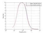
Here's a comparison of the correct transfer function (blue) with the transfer function shown in the OP's figure (red):

attachment.php


And here is a plot of both transfer functions with CL 100 times smaller:

attachment.php
 

Attachments

  • Tranf.png
    Tranf.png
    6.4 KB · Views: 283
  • Plot3.png
    Plot3.png
    20.2 KB · Views: 291
  • Plot4.png
    Plot4.png
    19.3 KB · Views: 284

    V

    Points: 2
    Helpful Answer Positive Rating
I can't follow at first sight how the 3rd order s term is eliminated in your expression.

Regarding transfer functions with high gain/low CL values, they possibly exceed the range where OTA output impedance can be neglected. A lower CL limit is also set by transistor technology, because it includes the output capacitance.
 

Re: Transfer function & high cutoff frequency

It's obviously not correct. With "qualitatively right", I meaned that it's giving giving a correct picture under some presumptions, e.g. CL >>C2.

Checking further, I see that even with CL 100 times greater than C2, the transfer function in the OP's figure is not giving a correct picture:

attachment.php


- - - Updated - - -

I can't follow at first sight how the 3rd order s term is eliminated in your expression.

Factoring the numerator and denominator of the SAPWIN result shows that there is a common factor in both (assuming I didn't make any mistakes when typing it all in). Removing that factor and using the remaining terms gives the reduced result.

attachment.php
 

Attachments

  • Plot5.png
    Plot5.png
    19.1 KB · Views: 278
  • Factor.png
    Factor.png
    8.7 KB · Views: 300
  • Like
Reactions: FvM

    FvM

    Points: 2
    Helpful Answer Positive Rating
    V

    Points: 2
    Helpful Answer Positive Rating
The given transfer function is valid only under certain condition. Some observations

1) Even though there are three capacitances C1 ,C2 and CL, it will be a second order system (as pointed earlier) as the the capacitances are in series and hence only two independent conditions can be specified.
2) There are two poles in the system (fl and fh in the graph) and they are widely separated. fh>>fl.
3) One of the pole is given by 1/(2*pi*R2*C2)
4) The second pole comes at the output of the transconductor. Total capacitance at the output is approx CL. The input conductance looking into the output of the transconductor is Gm scaled by voltage divider formed by C1 and C2. So the conductance is C2*Gm/(C1+C2). The pole comes at fh under the condition CL>>C1>>C2. Under this condition transfer function should be valid.
 

Checking further, I see that even with CL 100 times greater than C2, the transfer function in the OP's figure is not giving a correct picture
I agree that there isn't left much of an approximate correctness. For the high frequency gain, you get an additional factor two (C2/2CL) and so on. Furthermore any simplifications applied in analysis should be clearly mentioned.

Thanks for showing the factorization. SAPWIN in fact doesn't it.
 

The given transfer function is valid only under certain condition.

Why not just use a transfer function that is valid under all conditions? If the transfer function from post #1 were very much simpler than the correct transfer function, that might be a reason to use it. But the correct transfer function is not much more complicated, if any, and is always valid.

Some observations

1) Even though there are three capacitances C1 ,C2 and CL, it will be a second order system (as pointed earlier) as the the capacitances are in series and hence only two independent conditions can be specified.
2) There are two poles in the system (fl and fh in the graph) and they are widely separated. fh>>fl.
3) One of the pole is given by 1/(2*pi*R2*C2)
4) The second pole comes at the output of the transconductor. Total capacitance at the output is approx CL. The input conductance looking into the output of the transconductor is Gm scaled by voltage divider formed by C1 and C2. So the conductance is C2*Gm/(C1+C2). The pole comes at fh under the condition CL>>C1>>C2. Under this condition transfer function should be valid.
Here's a plot with CL = 100 C1, and C1 = 100 C2. The transfer function from the OP's post #1 is in red and the correct transfer function is in blue. I leave it up to the reader to decide if the transfer function from post #1 is valid.

attachment.php
 

Attachments

  • Plot6.png
    Plot6.png
    19.1 KB · Views: 268
  • Like
Reactions: FvM

    FvM

    Points: 2
    Helpful Answer Positive Rating
    V

    Points: 2
    Helpful Answer Positive Rating
An approximate transfer function gives an intuitive understanding of the location of poles and zeros. Thus there location can be found by just looking at the circuit , without doing much maths.
To have reasonable passband fh>>fl gives Gm*R2>>C1*CL/(C2*C2).

Also under the condition C1 and CL >> C2, the said transfer function is a reasonable approximation.
C1=CL=1e-6; C2=C1/10; Gm=1/10; R2=10e5.plot1.jpg
 

In post #10, you said:

The pole comes at fh under the condition CL>>C1>>C2. Under this condition transfer function should be valid.

and I gave a counterexample in post #12.

Now you give different conditions which do in fact produce similar results from the correct and incorrect transfer functions for particular component values.

An approximate transfer function gives an intuitive understanding of the location of poles and zeros. Thus there location can be found by just looking at the circuit , without doing much maths.
To have reasonable passband fh>>fl gives Gm*R2>>C1*CL/(C2*C2).

Also under the condition C1 and CL >> C2, the said transfer function is a reasonable approximation.
C1=CL=1e-6; C2=C1/10; Gm=1/10; R2=10e5.View attachment 91631

An approximate transfer function is fine provided that it's correct. The one from the original post is only a good approximation over a limited range.

This value for CL represents very heavy loading on the OTA, and the passband isn't very flat. I suppose it's possible that the circuit is intended to be heavily loaded, but the response curve in the figure of post #1 shows a substantial flat midband response. I don't think it's possible to get an extended flat midband response with component values that allow the transfer function from post #1 to closely approximate the correct response.

If we reduce CL by a factor of 50, probably a more realistic load, it's still true that "Gm*R2>>C1*CL/(C2*C2)". The original transfer function now deviates considerably from the correct one even though the condition is satisfied (and we have a flatter passband):

attachment.php


Reducing CL by 100 leads to this:

attachment.php


And reducing it by 200 leads to this:

attachment.php


These would be reasonable loads. The incorrect transfer function gives very bad results. I just don't see any value in the use of the original, incorrect, transfer function when the correct one is hardly more complicated.

I also discovered earlier that under certain conditions the incorrect transfer function closely approximates the correct one, but it seems to me to be rather limited conditions that give this result.
 

Attachments

  • Plot9.png
    Plot9.png
    22.7 KB · Views: 256
  • Plot8.png
    Plot8.png
    22.3 KB · Views: 283
  • Plot7.png
    Plot7.png
    23.3 KB · Views: 251

    V

    Points: 2
    Helpful Answer Positive Rating
In post #10, you said:


If we reduce CL by a factor of 50, probably a more realistic load, it's still true that "Gm*R2>>C1*CL/(C2*C2)". The original transfer function now deviates considerably from the correct one even though the condition is satisfied (and we have a flatter passband):

attachment.php


Reducing CL by 100 leads to this:

attachment.php


And reducing it by 200 leads to this:

attachment.php


These would be reasonable loads. The incorrect transfer function gives very bad results. I just don't see any value in the use of the original, incorrect, transfer function when the correct one is hardly more complicated.

I also discovered earlier that under certain conditions the incorrect transfer function closely approximates the correct one, but it seems to me to be rather limited conditions that give this result.

In addition to the condition,Gm*R2>>C1*CL/(C2*C2), the other condition for the expression to be valid is that both C1 and CL >> C2. Examples you have taken do not satisfy these. If you do not want the constraint on CL (as in your examples), the approx transfer function has to be modified.( Replace the term CL*C1/(Gm*C2) in the second part of denominator with (CL*C1+C1*C2)/(Gm*C2) ).

The second term in the denominator of the approx expression comes due to the pole at the output formed by conductance C2*Gm/(C1+C2) and load CL+C1*C2/(C1+C2).
With C1>>C2, pole is at C2*Gm/(CL*C1+C1*C2) (the modified approx expression above). With further constraint of CL>>C2, comes the original approximation.
 

    V

    Points: 2
    Helpful Answer Positive Rating
How about the value for the high frequency gain? The exact value has been calculated in post #6 and #7, it's C1C2/(C1C2 + 2 CLC1 + 2 CLC2)

You hardly manage to make it C2/CL, at best you'll achieve C2/(2CL). That's the point where I stopped to "save" the equations in the original post.
 

In addition to the condition,Gm*R2>>C1*CL/(C2*C2), the other condition for the expression to be valid is that both C1 and CL >> C2. Examples you have taken do not satisfy these.

I am aware of this. I mentioned that one condition was still satisfied when I said "it's still true that 'Gm*R2>>C1*CL/(C2*C2)'.", and I wanted to show what would happen if CL was made smaller.

Your example has a huge 1 microfarad capacitor for CL which I suspect is unreasonable. I was showing that if a more reasonable load is present, the incorrect transfer function fails badly even when the condition "Gm*R2>>C1*CL/(C2*C2)" is satisfied. The response curve in the original post shows a wide flat response which is not what is obtained over the limited range where the incorrect transfer function approximately matches the correct one. A flat midband response is apparently what is wanted, and is only obtained for much lighter loading than 1 microfarad, and over the lightly loaded range, the incorrect transfer function is not good.

If you do not want the constraint on CL (as in your examples), the approx transfer function has to be modified.( Replace the term CL*C1/(Gm*C2) in the second part of denominator with (CL*C1+C1*C2)/(Gm*C2) ).

Why bother making changes to the incorrect transfer function to make it "approximately" correct for some different range of component values when the correct transfer function works everywhere.

I continue to believe that there is no advantage to using the incorrect transfer function when the correct one is not very complicated, especially when the incorrect one fails so badly with more reasonable component values.

Maybe once upon a time there was a reason to avoid additional math, but not any more. Extensive math is not difficult given the ubiquitous computers in the world today. The math involved with this problem isn't all that difficult anyway; even my hand-held calculator can solve this problem symbolically.

I wonder if the OP has been following all this, and if it has been of any help?
 
  • Like
Reactions: FvM

    FvM

    Points: 2
    Helpful Answer Positive Rating
    V

    Points: 2
    Helpful Answer Positive Rating
Wow, I have pretty much the same problem! But I don't really understand how you get to your solution, is there a structured way to come to the transfer function? why is there a s^2 in the numerator? I did just use that formula:
TF = -(Z2/Z1)*1/(1 + 1/A + Z2/(Z1*A)) and use Z1 = 1/(s*C1); Z2 = (1/R + s*C2)^-1; A = gm/(CL*s)
but then I won't get the same result as you do... ;__;
here is my result: -((C1 gm R s)/(gm + C2 gm R s + CL s (1 + C1 R s + C2 R s)))
 

I performed a nodal analysis. There are 5 nodes in this circuit. The input is differential, so I applied a voltage Vin with a Thevenin resistance of Rs between nodes 1 and 2. Nodal analysis is easier with current sources, so I converted the input source to a current source with a value of Vin/Rs. After solving for the voltage at the output node (node 5 in my analysis), I took the limit as Rs -> 0.

Here is the admittance matrix form of the nodal equations operated on by a linear solver:

attachment.php


The output is a voltage vector of the 5 node voltages; the voltage at node 5 is the output voltage. That result is an expression multiplying Vin and the expression is the transfer function.

Why would you not expect s^2 in the numerator?
 

Attachments

  • Gm Prob.png
    Gm Prob.png
    18.5 KB · Views: 271

    V

    Points: 2
    Helpful Answer Positive Rating
Wow O.O I would never have come to such a solution but I will try to understand it, perhaps I will ask you again while working through it (it looks quite complex). In any case you really helped me a lot, so thank you very very much!
 

Status
Not open for further replies.

Similar threads

Part and Inventory Search

Welcome to EDABoard.com

Sponsor

Back
Top