Akshe
Junior Member level 2
Subthreshold bandgap reference design
Hi All,
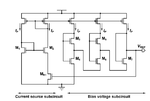
I am new to design and have been working on designing a low power bandgap reference circuit using subthreshold transistors for my college project. The design is based on a reference paper and i am trying to implement it on a different technology node. But i am unable to achieve the desired results.
I believe i am unable to size the devices appropriately and hence not getting the expected results. Currently i have tried two approaches for sizing - 1) Using the mentioned sizes in the paper 2) Starting from some scratch values and trying to use the equation to match the values. But with both i am unable to get results.
The design is as below:

Ref. Paper - JSSC Jul 09 - A 300 nW 15 ppmC 20 ppmV CMOS Voltage Reference Circuit Consisting of Subthreshold MOSFETs
View attachment JSSC Jul 09 - A 300 nW 15 ppmC 20 ppmV CMOS Voltage Reference Circuit Consisting of Subthreshold.pdf
Technology and specifications - 130nm process, BSIM4 model, Supply voltage- 0.9-1.5 V, 1.2V transistors
According to calculations and as per threshold modelling in BSIM4 the corresponding reference voltage should be nearly around 560mV.
The results that i obtain with the two approaches are as seen in the images..
1) Using Paper sizes


2) Using sizes from scratch


It would be of immense help to me if someone could help me in progressing with this as i have been stuck with this for a very long time now :sad:
Hi All,
I am new to design and have been working on designing a low power bandgap reference circuit using subthreshold transistors for my college project. The design is based on a reference paper and i am trying to implement it on a different technology node. But i am unable to achieve the desired results.
I believe i am unable to size the devices appropriately and hence not getting the expected results. Currently i have tried two approaches for sizing - 1) Using the mentioned sizes in the paper 2) Starting from some scratch values and trying to use the equation to match the values. But with both i am unable to get results.
The design is as below:

Ref. Paper - JSSC Jul 09 - A 300 nW 15 ppmC 20 ppmV CMOS Voltage Reference Circuit Consisting of Subthreshold MOSFETs
View attachment JSSC Jul 09 - A 300 nW 15 ppmC 20 ppmV CMOS Voltage Reference Circuit Consisting of Subthreshold.pdf
Technology and specifications - 130nm process, BSIM4 model, Supply voltage- 0.9-1.5 V, 1.2V transistors
According to calculations and as per threshold modelling in BSIM4 the corresponding reference voltage should be nearly around 560mV.
The results that i obtain with the two approaches are as seen in the images..
1) Using Paper sizes


2) Using sizes from scratch


It would be of immense help to me if someone could help me in progressing with this as i have been stuck with this for a very long time now :sad: