Continue to Site

Welcome to EDAboard.com

Welcome to our site! EDAboard.com is an international Electronics Discussion Forum focused on EDA software, circuits, schematics, books, theory, papers, asic, pld, 8051, DSP, Network, RF, Analog Design, PCB, Service Manuals... and a whole lot more! To participate you need to register. Registration is free. Click here to register now.

subc connection, it is not right?

Status
Not open for further replies.

shanmei

Advanced Member level 1
Joined
Jul 26, 2006
Messages
430
Helped
8
Reputation
16
Reaction score
8
Trophy points
1,298
Location
USA
Activity points
4,496
From the thread, https://www.edaboard.com/threads/264917/

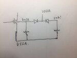
which shows NMOS bulk and sub! connection.
1.JPG

I am wondering the whether the connection is right. The trip well NMOS device is used to isolate the bulk node and the noisy sub! node. In the above figure, the bulk and sub! are actually shorted together though the subc.

1. Then how can the bulk immune from the noisy sub!?
2. We can assume that the two terminals of the subc are short, right?

Thanks.
 

ad1. Note, that bulk terminal and substrate are connected through contacts and metal layer to ground potential (low impedance node forcing well defined potential). Between transistor body and chip substrate are two reversed diodes and this makes the job. You could saw it better with schematic for nfet with source terminal not connected to the ground.
ad2. Yes, in this example both nfet bulk and chip substrate are connected by metal paths together to VSSA node.
 
The schematic of course is too simple to show the
reality of that routing and the routing of any noise
currents. Global nets are fine for circuits where this
does not matter. If you care, then care enough to
model such things at sufficient detail.
 
Thanks. Now I understand it is because the VSSA is a low impedance node which forces the potential at bulk to be zero.
 

Status
Not open for further replies.

Part and Inventory Search

Welcome to EDABoard.com

Sponsor

Back
Top