mburakbaran
Member level 2
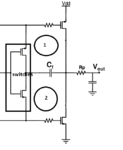
Hello, I am designing a slew-rate controlled digital output driver. The simplified output stage is attached. The feedback is done via the capacitor at the picture from output to a switching nodes. You can see the two switch transistors in rectangular.
Here, I am also adding series resistors to the gates of the output transistors in order to filter out some EMI that might be coupled inside. The output transistors are pretty big (around 5mm width fro the pmos e.g.) so adding a series resistor basically forms a Low pass RC. Anyway, my question is, how can I analyze the stability of these two feedback loops shown in circles? I mean I am doing transient simulations and all and everything seems ok, but what should I do to make sure that this will operate stable? I do not know about cutting the loops and applying sth from somewhere and stuff. Could somebody be help with this?
Much appreciated and thanks a lot.