Continue to Site

Welcome to EDAboard.com

Welcome to our site! EDAboard.com is an international Electronics Discussion Forum focused on EDA software, circuits, schematics, books, theory, papers, asic, pld, 8051, DSP, Network, RF, Analog Design, PCB, Service Manuals... and a whole lot more! To participate you need to register. Registration is free. Click here to register now.

[SOLVED] SMD FET soldering issue

Status
Not open for further replies.

Cval

Junior Member level 1
Joined
Jan 23, 2012
Messages
19
Helped
0
Reputation
0
Reaction score
0
Trophy points
1,281
Activity points
1,442
I am trying to solder a SMD FET to my PCB, this is a different fet than the PCB was originally designed for (Drain and Source switched places). When i solder it up like this the R1 on my PCB ignites. Is there a reason you cant solder SMD FETs like this?

I also tried to solder the through hole version of the original FET to the board and the same thing happened...
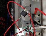

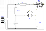
FETsldr.jpg
 

You are obviously connecting something wrong. With no schematic, I can't tell you anything else. HOW ARE WE SUPPOSED TO KNOW WHAT R1 IS??????
 

I didn't think it had anything to do with the layout, i figured it had more to do with the way I soldered the SMD FET. The source, gate, and drain are all in the correct positions. Attached is the schematic.

clschem.png

- - - Updated - - -

And here's the fet layout, I am attempting to connect the "new" fet in the "old" fet pad layout.

FETs.png
 

Do you mind to mention the MOSFET type? The switched pins thing sounds really unlikely.
 

How about some values? Voltages? What's connected to the connector? You are making this extremely difficult.
 

Status
Not open for further replies.

Part and Inventory Search

Welcome to EDABoard.com

Sponsor

Back
Top