Continue to Site

Welcome to EDAboard.com

Welcome to our site! EDAboard.com is an international Electronics Discussion Forum focused on EDA software, circuits, schematics, books, theory, papers, asic, pld, 8051, DSP, Network, RF, Analog Design, PCB, Service Manuals... and a whole lot more! To participate you need to register. Registration is free. Click here to register now.

[SOLVED] Sine wave inverter with pic16f72 and if2110

Status
Not open for further replies.

EZEROBERT

Newbie
Newbie level 3
Joined
Mar 29, 2013
Messages
3
Helped
1
Reputation
2
Reaction score
1
Trophy points
1,283
Visit site
Activity points
1,456
Please sir i want the link of this ckt and to get more understand about it and the hex file
 

Attachments

  • my inv pic16f72.pdf
    1.3 MB · Views: 2,250

if you do a web search for pure sine inverter control circuit and similar you will find plenty of discussion on sine wave inverter cuircuits
 
  • Like
Reactions: giovanniester

    giovanniester

    Points: 2
    Helpful Answer Positive Rating
    V

    Points: 2
    Helpful Answer Positive Rating
Dear Ezerobert,/Readers
You can use the code, in the attached file.

All best
Mohamad Rahman.
 

Attachments

  • sine_tech_mail.rar
    2.5 MB · Views: 2,113
Dear MRahman sir

Thanks for your nice Attached file. I read full documents.

I try to make project by using MPLAB ASM , but there is lot of error. Please tell me which compiler used for "sn3_ups".

Also, I try to open "SINE_03 PCB File" but can not open. Please tell me which PCB design software used for "SINE_03 PCB File".

Sir, I am waiting for your kind replay.

please ..............

- - - Updated - - -

Dear MRahman sir

I found small similarity with CCS C compiler with your "sn3_ups". if program is written in CCS C compiler Please send me "sn3_ups.c". anowar.mieb26234@gmail.com
 

Dear MRahman sir

Can you please the charging path , when high side MOSFET are off .........

- - - Updated - - -

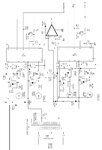
<a title="sine_ckt_0004.jpg" href="http://obrazki.elektroda.pl/1827625300_1426652419.jpg"><img src="http://obrazki.elektroda.pl/1827625300_1426652419_thumb.jpg" alt="sine_ckt_0004.jpg" /></a>

- - - Updated - - -

sine_ckt_0004.jpg Can you please the charging path , when high side MOSFET are off .........
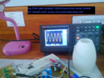
 

In My proteus Simulation Sign wave is not stable. Inverter Run on Square wave but MPLAB simulation shows it takes values from Sign Table but output is square wave. help me please about ccp1.
 

Attachments

  • edaboard.rar
    120.4 KB · Views: 889

Hey Arif.

try and understand the way it works. the sign waves had been chopped into discrete numbers of 1 and 0 in time. so what you will have is a square wave as the output pin of the micro can either be one(1) or Zero(0). so by using a low pass filter at the output. you get sinewave output. if all is ok with your design.

hope this helps

tunde
 

Dear MRahman sir

Thanks for your nice Attached file. I read full documents.

I try to make project by using MPLAB ASM , but there is lot of error. Please tell me which compiler used for "sn3_ups".

Also, I try to open "SINE_03 PCB File" but can not open. Please tell me which PCB design software used for "SINE_03 PCB File".

Sir, I am waiting for your kind replay.

please ..............

- - - Updated - - -

Dear MRahman sir

I found small similarity with CCS C compiler with your "sn3_ups". if program is written in CCS C compiler Please send me "sn3_ups.c".


please send the "sn3_ups.c"

.. regarding the compiltion with mplab -- it has
too many error, but inverter is working well, try to understand how the inverter works, then it will be easier for you to implement. thanks Mrahman.. please send me a copy of sn3_ups.c thank you
regard .. henry Nigeria.
 
Last edited by a moderator:

Dear Ezerobert,/Readers
You can use the code, in the attached file.

All best
Mohamad Rahman.

Thanks for sharing, really appreciate this. But please i would love if u can help clear some doubt.

1. What are the terminal voltage of the transformers(the primary and the secondary when not used in the inverter circuit.
for the 24 volt version is 230 to 24v or 230 to 16v. considering the peak value of the battery voltage.

2. please can you explain how the feedback loop works with the voltage compensation. (how does the sinetable compensate for low or high output voltage.

3. how many times do u sample the feedback circuit and how long do u do compensation for the output voltage regulation.

thanks.

tunde
 

Dear all,

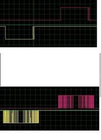
Sign PWM looks like first picture in simulation but it may be looks like second picture, help me for adjustment .........


<a title="Sign PWM Shap.jpg" href="http://obrazki.elektroda.pl/1775463800_1427870451.jpg"><img src="http://obrazki.elektroda.pl/1775463800_1427870451_thumb.jpg" alt="Sign PWM Shap.jpg" /></a>

- - - Updated - - -


Hi Ariff;

are this the outputs from the logic gates,or the gate drivers?

if the second waveform is from the logic gate. i would say is ok and i could see sometime time difference between the two. that is good as its a means of good dead time between the mosfets when they switch.

tunde
 

Hello every one,
I try to do a practical simulation of this inverter but the feedback is not working. Has any body successfully implemented this inverter . see my attached simulation in the image below.IMG_20150402_164837.jpg
 

the feedback is not working also in simulation ......

We needs some help from MPLAB asm expert to solve this ccp1 problem ....
 

The circuit M Rahman post has some errors but the code was ok and the inverter is working very well i advice members to study circuit diagram first and understand how it works before building it
 
Dear adamhenry and kabeer02


Please, help me and us by sharing your knowledge.How to solved this feedback problem?

We are waiting for kind replay ...........
 

Status
Not open for further replies.

Part and Inventory Search

Welcome to EDABoard.com

Sponsor

Back
Top