Continue to Site

Welcome to EDAboard.com

Welcome to our site! EDAboard.com is an international Electronics Discussion Forum focused on EDA software, circuits, schematics, books, theory, papers, asic, pld, 8051, DSP, Network, RF, Analog Design, PCB, Service Manuals... and a whole lot more! To participate you need to register. Registration is free. Click here to register now.

simultanius powering two opamp devices question

yefj

Advanced Member level 4
Joined
Sep 12, 2019
Messages
1,245
Helped
1
Reputation
2
Reaction score
3
Trophy points
38
Activity points
7,508
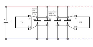
Hell i have a single 5V DC power sourse for two opamps.
the problem is we both opamps open we have a double load so if i connect in parralel my power suplly then my current will be half for each opamp.
given the data sheet bellow,each opamp needs 80uA current,so i put 160uA on my power suply
How do i know the minimal trace width/tickness i need it could sustain this 160uA current threw it?
Thanks.

1688747846472.png
 
Sorry FVM, it wont happen again,i am new to this field and i will post to the proper forum.
--- Updated ---

Hi,

What are you asking for?
How to connect all "+" and how to connect all "-"?
Where is the problem?

Maybe there is some difficulty or requirement that I don't see ... but basically it's as simple as connectiong three [LEDs with resistor] in parallel to a single battery.

Klaus
Hello Klauss ,My problem is if i will take a 3 pin connector (plus ,minus ,ground)
i will have the situation where one amplifier is closer then the other.
so i have the following issues.
1.the trace width in the current amplifier suited for the power of a single amplifier.
I have a main artery which will have 4 times more power then that.
How do i know what trase dimentions to use so it could handle the power flowing threw it?

2.i need to make sure every power amplifier get equal voltage

In the QORVO amplifier they put the RF feeding and DC feeding in the same layer for one amplifier.
Looking at the PCB layers is it possible to feed in parraler bit RF and DC?
Thanks.
1691038876731.png

1691039126991.png

1691039056835.png
.
 
Last edited:
Hi,

I´m really confused. You talk like you have to supply each OPAMP with 100A or so, and you have to care about voltage drop and overheating the trace...
But it´s just a couple of mA, isn´t it? So we are talking about microVolts of drop and nanoWatts to be dissipated...

It´s all said in the thread above. If you don´t read the posts ... it´s useless to answer you!

Again: It´s just like connecteding some LEDs. Did you any time care about the voltage drop in a wire supplying a LED?
But if you are concerneed: Why don´t you just use an online tool for PCB trace calculations and they will show you the voltage drop and dissipation (temperature rise). (Btw: you should be able to calculate the same by hand)
On the other hand: What makes you think to use the minumum trace with. Just use a wide trace and all your concernes don´t exist anymore. Or use a supply plane.

1.the trace width in the current amplifier suited for the power of a single amplifier.
I have a main artery which will have 4 times more power then that.
This sounds as if you are able to calculate the trace width for the current of a single amplifier .. but unable to do the same for the current of 4 amplifiers. Makes no sense! If (again: IF) this is over your head, then doing electronics design will be a very hard job for you.

2.i need to make sure every power amplifier get equal voltage
Basic question:
* WHY do they need to be equal?
* and what does "equal" mean to you. While it it easy to say that "2 = 2" and "2 unequal 3" when using with digital numbers. But doing the same with analog values is basically impossible. There will always be a difference. Difference in the range of picoVolts .. or difference in time .. at least when yoou take noise into consideration.

So you have to define what "equal" means (at least for yourself). How much deviation do you allow in the supply voltage of your OPAMPs? picoVolts? nanoVolts? microVolts? milliVolts?

What do expect will happen if one OPAMP´s supply is +4.9876V while at the other OPAMP it is 4.8123V?
(just random values)

If you are concerned that OPAMPs will "operate differently" .. then how do you overcome the fact that they will "operate differently" just because fo production tolerances?

In the QORVO amplifier they put the RF feeding and DC feeding in the same layer for one amplifier.
Looking at the PCB layers is it possible to feed in parraler bit RF and DC?
Now you switch over to RF. A complete different topic.
DC supply routing is as far from RF signal routing as can be.
* with DC routing you (mainly) care about voltage drop and heat, basically caused by ohmi loss of the trace. You can´t go wrong using wider traces.
* with RF you (mainly) are concerened about charactereistic trace impedance, delay, EMI, EMC, HF loss. You have to carre about trace width, core thickness, nearby traces....

With DC there is no impedance! It´s just pure ohmic resistance.
The only thing to keep in mind: use a suitable decoupling capacitor at the point of load (OPAMPs), so that the remaining (unavoidable) AC is low in frequency and low in level. But this is not a difficult nor an extra task, it should be standard to put suitable decoupling capacitors at each supply pin of each IC.

Klaus
 
HEMT RF Amp ? There are Gerber files to work from, and I see its in the order of
3A drain current per amp so if you are paralleling several of these you will have
to pay attention to bussing of that as well as layout and matching of the other amps.

There is a fair amount of design methodology and practices in this :


Also I would contact QORVO tech support with these questions....


Regards, Dana.
 
Last edited:
Hi,

HEMT RF amp, 3A...

my mistake. I still was with the couple of mA of the AD8031 ..

But the physics and math is the same....

Klaus
 
Hi yefj,

Rule-of-thumb for the decoupling capacitors: Large value closest to supply rail, small value closest to IC supply pins. Small value capacitor absorbs fast transient dips/supplies fast current to the IC, the large value is a reservoir capacitor buffering the rest of circuit from the IC's transients.
 

Attachments

  • Capacitor placement vs capacitor value and IC and supply rails.jpg
    Capacitor placement vs capacitor value and IC and supply rails.jpg
    75.8 KB · Views: 65

LaTeX Commands Quick-Menu:

Part and Inventory Search

Welcome to EDABoard.com

Sponsor

Back
Top