Continue to Site

Welcome to EDAboard.com

Welcome to our site! EDAboard.com is an international Electronics Discussion Forum focused on EDA software, circuits, schematics, books, theory, papers, asic, pld, 8051, DSP, Network, RF, Analog Design, PCB, Service Manuals... and a whole lot more! To participate you need to register. Registration is free. Click here to register now.

[SOLVED] Simulating Semi-floating gate current mirror using HSPICE

Status
Not open for further replies.

deardeepa76

Junior Member level 3
Joined
Dec 8, 2011
Messages
29
Helped
0
Reputation
0
Reaction score
0
Trophy points
1,281
Activity points
1,491
Dear All,

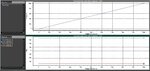
I am trying to simulate a semi-floating gate current mirror seen in fig1.
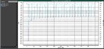
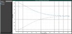
How to get the graph as output, what sweep should I make?

Fig 1
Capture.JPG Capture1.JPG
This is the netlist

Code:
* CSFG Common gate current mirror recharge freq 100MHz

********* Simulation Settings - General section *********
.include "D:\HSPICE\NewCSFGBkup\t96w_9sf_9m_lb_3-params.txt"

********* Simulation Settings - Parameters and SPICE Options *********

*-------- Devices: SPICE.ORDER > 0 --------
CCinn V1 N_3  1p  
CCinp1 In N_4  1p  
CCinp2 Out N_5  1p  
MNMOS_1 V1 N_3 Vdd1 Gnd CMOSN W=2.5u L=250n AS=2.25p PS=6.8u AD=2.25p PD=6.8u  
MNMOS_2 Out N_3 Vdd1 Gnd CMOSN W=2.5u L=250n AS=2.25p PS=6.8u AD=2.25p PD=6.8u  
MNMOS_3 N_4 Vdd1 Gnd Gnd CMOSN W=2.5u L=250n AS=2.25p PS=6.8u AD=2.25p PD=6.8u  
MNMOS_4 N_5 Vdd1 Gnd Gnd CMOSN W=2.5u L=250n AS=2.25p PS=6.8u AD=2.25p PD=6.8u  
MPMOS_1 N_3 Vdd2 Vdd Vdd CMOSP W=2.5u L=250n AS=2.25p PS=6.8u AD=2.25p PD=6.8u  
MPMOS_2 V1 N_4 Vdd2 Vdd CMOSP W=2.5u L=250n AS=2.25p PS=6.8u AD=2.25p PD=6.8u  
MPMOS_3 Out N_5 Vdd2 Vdd CMOSP W=2.5u L=250n AS=2.25p PS=6.8u AD=2.25p PD=6.8u  
VVsupply Vdd Gnd  DC 250m 
VVf Vdd1 Gnd  PULSE(0 1 0 3n 3n 10n 40n)  
VVfbar Vdd2 Gnd  PULSE(0 1 20n 3n 3n 10n 40n)   
VVin In Gnd  DC 1 SIN(.125 .125 2MEG) 

********* Simulation Settings - Analysis section *********
.tran 100n 2u
.DC VVin  0 250m .0250
.print dc ID(MPMOS_2)
.print dc ID(MPMOS_3)

********* Simulation Settings - Additional SPICE commands *********

.end
 

How to get the graph as output,
Depends on your graphical output tool.
what sweep should I make?

The sweep is already contained in your netlist:
Code:
.DC VVin  0 250m .0250
If you want to change it to the conditions of Fig. 5 , change
Code:
VVsupply Vdd Gnd  DC 250m
to
Code:
VVsupply Vdd Gnd  DC 175m
and
Code:
.DC VVin  0 250m .0250
to
Code:
.DC VVin  100m 0 10m
.
 

Hi erikl,
thanks for the response. When I am sweeping VVin in that range, the current is found to be constant at 171.840fA, not like what I see in Fig5.
I simulated using HSPICE and I have attached the outputscreen for reference.
 

Attachments

  • Capture.JPG
    Capture.JPG
    260.2 KB · Views: 119

What are the threshold voltages of your MOSFETs? Perhaps you could present their model files, or a link to them?
 

I see some confusion about simulation setup. You are performing a DC sweep of a voltage source that's capacitively coupled to the active circuit. Respectively, there's no effect on any circuit current.

As a first step, consider what you want to achieve, possibly a parametric sweep in transient analysis?

Thanks FvM, I tried doing a parameter sweep in transient analysis, I have attached the screen shot below. The current in pulsating, but I expect a linear increase as in original
The netlist is

Code:
* CSFG Common gate current mirror recharge freq 25MHz

********* Simulation Settings - General section *********
.include "D:\HSPICE\NewCSFGBkup\t96w_9sf_9m_lb_3-params.txt"
.param vin_param=1V

********* Simulation Settings - Parameters and SPICE Options *********

*-------- Devices: SPICE.ORDER > 0 --------
CCinn V1 N_3  1p  
CCinp1 In N_4  1p  
CCinp2 Out N_5  1p  
MNMOS_1 V1 N_3 Vdd1 Gnd CMOSN W=2.5u L=250n AS=2.25p PS=6.8u AD=2.25p PD=6.8u  
MNMOS_2 Out N_3 Vdd1 Gnd CMOSN W=2.5u L=250n AS=2.25p PS=6.8u AD=2.25p PD=6.8u  
MNMOS_3 N_4 Vdd1 Gnd Gnd CMOSN W=2.5u L=250n AS=2.25p PS=6.8u AD=2.25p PD=6.8u  
MNMOS_4 N_5 Vdd1 Gnd Gnd CMOSN W=2.5u L=250n AS=2.25p PS=6.8u AD=2.25p PD=6.8u  
MPMOS_1 N_3 Vdd2 Vdd Vdd CMOSP W=2.5u L=250n AS=2.25p PS=6.8u AD=2.25p PD=6.8u  
MPMOS_2 V1 N_4 Vdd2 Vdd CMOSP W=2.5u L=250n AS=2.25p PS=6.8u AD=2.25p PD=6.8u  
MPMOS_3 Out N_5 Vdd2 Vdd CMOSP W=2.5u L=250n AS=2.25p PS=6.8u AD=2.25p PD=6.8u  
VVsupply Vdd Gnd  DC 175m 
VVf Vdd1 Gnd  PULSE(0 1 0 3n 3n 10n 40n)  
VVfbar Vdd2 Gnd  PULSE(0 1 20n 3n 3n 10n 40n)   
VVin In Gnd  DC vin_param SIN(.125 .125 2MEG) 

********* Simulation Settings - Analysis section *********
.tran 100n 1u  sweep VVin 100m  0 10m $linear sweep

.print tran ID(MPMOS_2)
.print tran ID(MPMOS_3)
.print tran ID(MNMOS_1)
.print tran ID(MNMOS_2)

********* Simulation Settings - Additional SPICE commands *********

.end
 

Attachments

  • Capture.JPG
    Capture.JPG
    414.4 KB · Views: 114

1. Considering the threshold voltages of this process, I think your power supply is too low. I'd suggest to increase it to perhaps 1V - that's the voltage you give to the clocking signals phi, phibar :
Code:
VVsupply Vdd Gnd  DC 1

2. As FvM pointed out above, it doesn't make much sense to sweep the DC input voltage at Vin, as it is capacitively coupled to the circuit. The sinusoidal "sweep" at this node might be enough for this purpose:
Code:
VVin Vin Gnd  SIN(0 .500 2MEG)

If not, I guess you could sweep the voltage @ node V1 instead - and with different values, then:
Code:
VV1 V1 Gnd DC 0
.tran 1n 1u  sweep VV1 500m  0 100m $linear sweep


The current in pulsating, but I expect a linear increase as in original

Of course these currents are pulsating, because you are chopping them (phi, phibar). In order to get this relationship between Ie1, Ie2 and Iin, you have to extract the respective maximum values.
 
Hi erikl, thanks for the response. Regarding the power supply, the objective is to design the current mirror for Ultra-Low-Voltage. I have attached the base paper I am trying to implement here(Fig 3). So, the supply voltage is 175mV as mentioned in the paper.
 

Attachments

  • 2008-Clocked semifloating-gate ultra low-voltage current mirror.pdf
    335.7 KB · Views: 49

So, the supply voltage is 175mV as mentioned in the paper.

Hi dear deepa, thank you for the paper! May I cite from it (I. INTRODUCTION):

1. Supply voltage:
It is necessary that the analog power supply be at least equal to the sum of the magnitudes of the n-channel and p-channel thresholds.
So, the supply voltage with your MOSFETs should be ≧ 450mV , taking into account the VTH0 values of your model file - may be a bit less if you are working in weak inversion.

2. Sweeping:
The input Vin is swept from VDD/2 to gnd.
(2nd page, and Fig. 5). So:
.param v0=0 va='VDD/2' freq=0.5MEG delay=0 theta=0 phase=90
VVin Vin 0 sin(v0 va freq delay theta phase) $sinusoidal sweep
or:
VVin Vin Gnd DC 'VDD/2'
.tran 1n 1u sweep VVin 'VDD/2' 0 100m $linear sweep

3. Clocking frequency:
The recharge frequency is 100MHz
So you should perhaps adapt your clock frequency for phi, phibar.
 
Hi erikl, thanks a lot for the response. I have few questions in mind regarding the supply voltage.

1. Supply voltage:

So, the supply voltage with your MOSFETs should be ≧ 450mV , taking into account the VTH0 values of your model file - may be a bit less if you are working in weak inversion.
I agree to this but it is mentioned in the text of Fig5 that supply voltage VDD= 175mV as well as in last para of 2nd page. The abstract also says that the proposed current mirror can operate at supply voltages below 200mV.
Regarding the model file, I just downloaded it from mosis for 90nm and started using it, I am not sure about whether the threshold voltages mentioned there is correct for my simulation.

Regarding sweeping I did all the changes you have mentioned and here is the output screen shot and net list
Capture.JPG
Code:
* CSFG Common gate current mirror recharge freq 100MHz

********* Simulation Settings - General section *********
.include "D:\HSPICE\NewCSFGBkup\t96w_9sf_9m_lb_3-params.txt"
.param v0=0 va=225m freq=.5MEG delay=0 theta=0 phase=90

********* Simulation Settings - Parameters and SPICE Options *********

*-------- Devices: SPICE.ORDER > 0 --------
CCinn V1 N_3  1p  
CCinp1 In N_4  1p  
CCinp2 Out N_5  1p  
MNMOS_1 V1 N_3 Vdd1 Gnd CMOSN W=2.5u L=250n AS=2.25p PS=6.8u AD=2.25p PD=6.8u  
MNMOS_2 Out N_3 Vdd1 Gnd CMOSN W=2.5u L=250n AS=2.25p PS=6.8u AD=2.25p PD=6.8u  
MNMOS_3 N_4 Vdd1 Gnd Gnd CMOSN W=2.5u L=250n AS=2.25p PS=6.8u AD=2.25p PD=6.8u  
MNMOS_4 N_5 Vdd1 Gnd Gnd CMOSN W=2.5u L=250n AS=2.25p PS=6.8u AD=2.25p PD=6.8u  
MPMOS_1 N_3 Vdd2 Vdd Vdd CMOSP W=2.5u L=250n AS=2.25p PS=6.8u AD=2.25p PD=6.8u  
MPMOS_2 V1 N_4 Vdd2 Vdd CMOSP W=2.5u L=250n AS=2.25p PS=6.8u AD=2.25p PD=6.8u  
MPMOS_3 Out N_5 Vdd2 Vdd CMOSP W=2.5u L=250n AS=2.25p PS=6.8u AD=2.25p PD=6.8u  
VVsupply Vdd Gnd  DC 450m 
VVf Vdd1 Gnd  PULSE(0 5 0 .5n .5n 3.5n 10n)  
VVfbar Vdd2 Gnd  PULSE(0 5 5n .5n .5n 3.5n 10n)  
VVin In Gnd  DC 225m SIN(v0 va freq delay theta phase) $sinusoidal sweep

********* Simulation Settings - Analysis section *********
.tran 10n 100n  sweep VVin 225m  0 22.5m $linear sweep

.print tran ID(MPMOS_2)
.print tran ID(MPMOS_3)
.print tran ID(MNMOS_1)
.print tran ID(MNMOS_2)

********* Simulation Settings - Additional SPICE commands *********

.end
 

... regarding the supply voltage.
I agree to this but it is mentioned in the text of Fig5 that supply voltage VDD= 175mV as well as in last para of 2nd page. The abstract also says that the proposed current mirror can operate at supply voltages below 200mV.

I guess they used a process/transistors with lower threshold voltage values.

Regarding the model file, I just downloaded it from mosis for 90nm and started using it, I am not sure about whether the threshold voltages mentioned there is correct for my simulation.

With that higher Vsupply of 450mV it seems to work. The currents, however, are a bit high, so you could try and reduce Vsupply to maybe 200 .. 250mV to operate the transistors in weak inversion mode.

Regarding sweeping I did all the changes you have mentioned and here is the output screen shot and net list

Re. VVin: You don't need both sweeps (I said: "or"). If you run the linear sweep with the transient analysis, an additional sinusoidal sweep isn't necessary (however doesn't bother, because it's overrun by the transient sweep).
Code:
VVin In Gnd  DC 225m
would be enough.

Code:
.tran 10n 100n  sweep VVin 225m  0 22.5m $linear sweep
A single 100ns plot of currents doesn't give much info: you'd have to compare the max. currents for the 11 sweep runs.

BTW:
Code:
VVf Vdd1 Gnd  PULSE(0 5 0 .5n .5n 3.5n 10n)  
VVfbar Vdd2 Gnd  PULSE(0 5 5n .5n .5n 3.5n 10n)
The clock pulses should have the same height as Vsupply - not 5V - at least in reality.
 
I guess they used a process/transistors with lower threshold voltage values.
With that higher Vsupply of 450mV it seems to work. The currents, however, are a bit high, so you could try and reduce Vsupply to maybe 200 .. 250mV to operate the transistors in weak inversion mode.


BTW:
The clock pulses should have the same height as Vsupply - not 5V - at least in reality.

Hi erikl, thanks for the valuable inputs, I changed the clock pulse heights to VDD, after this change the current was reduced as seen in this screen shot
Capture.JPG

Code:
* CSFG Common gate current mirror recharge freq 100MHz VDD 450mV

********* Simulation Settings - General section *********
.include "D:\HSPICE\NewCSFGBkup\t96w_9sf_9m_lb_3-params.txt"
.param vdd=450m 

********* Simulation Settings - Parameters and SPICE Options *********

*-------- Devices: SPICE.ORDER > 0 --------
CCinn V1 N_3  1p  
CCinp1 In N_4  1p  
CCinp2 Out N_5  1p  
MNMOS_1 V1 N_3 Vdd1 Gnd CMOSN W=2.5u L=250n AS=2.25p PS=6.8u AD=2.25p PD=6.8u  
MNMOS_2 Out N_3 Vdd1 Gnd CMOSN W=2.5u L=250n AS=2.25p PS=6.8u AD=2.25p PD=6.8u  
MNMOS_3 N_4 Vdd1 Gnd Gnd CMOSN W=2.5u L=250n AS=2.25p PS=6.8u AD=2.25p PD=6.8u  
MNMOS_4 N_5 Vdd1 Gnd Gnd CMOSN W=2.5u L=250n AS=2.25p PS=6.8u AD=2.25p PD=6.8u  
MPMOS_1 N_3 Vdd2 Vdd Vdd CMOSP W=2.5u L=250n AS=2.25p PS=6.8u AD=2.25p PD=6.8u  
MPMOS_2 V1 N_4 Vdd2 Vdd CMOSP W=2.5u L=250n AS=2.25p PS=6.8u AD=2.25p PD=6.8u  
MPMOS_3 Out N_5 Vdd2 Vdd CMOSP W=2.5u L=250n AS=2.25p PS=6.8u AD=2.25p PD=6.8u  
VVsupply Vdd Gnd  DC vdd 
VVf Vdd1 Gnd  PULSE(0 vdd 0 .5n .5n 3.5n 10n)  
VVfbar Vdd2 Gnd  PULSE(0 vdd 5n .5n .5n 3.5n 10n)  
VVin In Gnd  DC 'vdd/2' 

********* Simulation Settings - Analysis section *********
.tran 10n 100n  sweep VVin 'vdd/2'  0 22.5m $linear sweep

.print tran ID(MPMOS_2)
.print tran ID(MPMOS_3)
.print tran ID(MNMOS_1)
.print tran ID(MNMOS_2)

********* Simulation Settings - Additional SPICE commands *********

.end

Capture.JPG
when I changed the VDD to 350mV, the output is this and below this voltage the current waveform was choppy and irregular. So I guess if I can get any other process/technology file with less VTH I can still reduce the VDD
 
Last edited:

when I changed the VDD to 350mV, the output is this and below this voltage the current waveform was choppy and irregular. So I guess if I can get any other process/technology file with less VTH I can still reduce the VDD

Right. Now if you want to get the Ie1, Ie2 vs. Iin dependency (Fig. 5.), extract the max. current values of these currents in the best possible steady state, say at 97.5ns of your sim. - you could do this with a .measure command - do this from all sweeps, which will give you different values for these currents from all these sweeps. Then plot these current values like Fig. 5. - either manually, or with the help of an Excel table, or with MATLAB.

BTW:
Code:
.tran 10n 100n  sweep VVin 'vdd/2' 0  [B]'vdd/20'[/B] $linear sweep
... will always give you 10 (resp. 11) sweep runs.
 
Right. Now if you want to get the Ie1, Ie2 vs. Iin dependency (Fig. 5.), extract the max. current values of these currents in the best possible steady state, say at 97.5ns of your sim. - you could do this with a .measure command - do this from all sweeps, which will give you different values for these currents from all these sweeps. Then plot these current values like Fig. 5. - either manually, or with the help of an Excel table, or with MATLAB.

Thanks erikl, I gave measure command and got the max values for Ie1 and Ie2 in measure results file for HSPICE. But these values are not different, I am not able to understand why. This is the results file View attachment measure.txt and the screenshot Capture.JPG
Code:
* CSFG Common gate current mirror recharge freq 100MHz

********* Simulation Settings - General section *********
.include "D:\HSPICE\NewCSFGBkup\t96w_9sf_9m_lb_3-params.txt"
.param vdd=450m 

********* Simulation Settings - Parameters and SPICE Options *********

*-------- Devices: SPICE.ORDER > 0 --------
CCinn V1 N_3  1p  
CCinp1 In N_4  1p  
CCinp2 Out N_5  1p  
MNMOS_1 V1 N_3 Vdd1 Gnd CMOSN W=2.5u L=250n AS=2.25p PS=6.8u AD=2.25p PD=6.8u  
MNMOS_2 Out N_3 Vdd1 Gnd CMOSN W=2.5u L=250n AS=2.25p PS=6.8u AD=2.25p PD=6.8u  
MNMOS_3 N_4 Vdd1 Gnd Gnd CMOSN W=2.5u L=250n AS=2.25p PS=6.8u AD=2.25p PD=6.8u  
MNMOS_4 N_5 Vdd1 Gnd Gnd CMOSN W=2.5u L=250n AS=2.25p PS=6.8u AD=2.25p PD=6.8u  
MPMOS_1 N_3 Vdd2 Vdd Vdd CMOSP W=2.5u L=250n AS=2.25p PS=6.8u AD=2.25p PD=6.8u  
MPMOS_2 V1 N_4 Vdd2 Vdd CMOSP W=2.5u L=250n AS=2.25p PS=6.8u AD=2.25p PD=6.8u  
MPMOS_3 Out N_5 Vdd2 Vdd CMOSP W=2.5u L=250n AS=2.25p PS=6.8u AD=2.25p PD=6.8u  
VVsupply Vdd Gnd  DC vdd 
VVf Vdd1 Gnd  PULSE(0 vdd 0 .5n .5n 3.5n 10n)  
VVfbar Vdd2 Gnd  PULSE(0 vdd 5n .5n .5n 3.5n 10n)  
VVin In Gnd  DC 'vdd/2' 

********* Simulation Settings - Analysis section *********
.tran 10n 100n  sweep VVin 'vdd/2'  0 'vdd/20' $linear sweep
.meas maxIe1 MAX I(MNMOS_1) from=97ns to=98ns
.meas maxIe2 MAX I(MNMOS_2) from=97ns to=98ns

********* Simulation Settings - Additional SPICE commands *********

.end
 
Last edited:

I gave measure command and got the max values for Ie1 and Ie2 in measure results file for HSPICE.
Good! But you need a third .meas command to measure Iin.

But these values are not different, ...
They should be. Your netlist looks like you didn't remove (or short-cut) Cinp1 for DC (i.e. non-RF) input (s. FvM's contribution #6 above). Cinp1 would just be ok for a sinusoidal input.

BTW:
(H)SPICE netlists usually need the node "0". May be this node is generated automatically by your simulation setup, but it wouldn't be amiss to insert a connection between Gnd and the 0 node:
Code:
Vgnd Gnd 0 DC 0
 
Good! But you need a third .meas command to measure Iin.

They should be. Your netlist looks like you didn't remove (or short-cut) Cinp1 for DC (i.e. non-RF) input (s. FvM's contribution #6 above). Cinp1 would just be ok for a sinusoidal input.

:grin:Finally I got it, thanks a lot erikl, your inputs was of utmost help to me. Thanks for taking u'r time and effort to help me out:grin:

Code:
* CSFG Common gate current mirror recharge freq 100MHz

********* Simulation Settings - General section *********
.include "D:\HSPICE\NewCSFGBkup\t96w_9sf_9m_lb_3-params.txt"
.param vdd=450m 

********* Simulation Settings - Parameters and SPICE Options *********

*-------- Devices: SPICE.ORDER > 0 --------
CCinn V1 N_3  1p  
*CCinp1 In N_4  1p  
CCinp2 Out N_5  1p  
MNMOS_1 V1 N_3 Vdd1 Gnd CMOSN W=2.5u L=250n AS=2.25p PS=6.8u AD=2.25p PD=6.8u  
MNMOS_2 Out N_3 Vdd1 Gnd CMOSN W=2.5u L=250n AS=2.25p PS=6.8u AD=2.25p PD=6.8u  
MNMOS_3 N_4 Vdd1 Gnd Gnd CMOSN W=2.5u L=250n AS=2.25p PS=6.8u AD=2.25p PD=6.8u  
MNMOS_4 N_5 Vdd1 Gnd Gnd CMOSN W=2.5u L=250n AS=2.25p PS=6.8u AD=2.25p PD=6.8u  
MPMOS_1 N_3 Vdd2 Vdd Vdd CMOSP W=2.5u L=250n AS=2.25p PS=6.8u AD=2.25p PD=6.8u  
MPMOS_2 V1 N_4 Vdd2 Vdd CMOSP W=2.5u L=250n AS=2.25p PS=6.8u AD=2.25p PD=6.8u  
MPMOS_3 Out N_5 Vdd2 Vdd CMOSP W=2.5u L=250n AS=2.25p PS=6.8u AD=2.25p PD=6.8u  
VVsupply Vdd Gnd  DC vdd 
VVf Vdd1 Gnd  PULSE(0 vdd 0 .5n .5n 3.5n 10n)  
VVfbar Vdd2 Gnd  PULSE(0 vdd 5n .5n .5n 3.5n 10n)  
VVin N_4 Gnd  DC 'vdd/2' 
Vgnd Gnd 0 DC 0

********* Simulation Settings - Analysis section *********
.tran 10n 100n  sweep VVin 'vdd/2'  0 'vdd/20' $linear sweep
.meas tran maxIe1 MAX I(MNMOS_1) from=97ns to=98ns
.meas tran maxIe2 MAX I(MNMOS_2) from=97ns to=98ns
.meas tran maxIin MAX I(MPMOS_2)  from=97ns to=98ns

********* Simulation Settings - Additional SPICE commands *********

.end
 

Attachments

  • Capture.JPG
    Capture.JPG
    205.2 KB · Views: 117

Congratulations, dear deepa!

Looks like a very good mirror symmetry between Ie1 & Ie2.
 

Hi erikl, I have another mirror circuit Fig 4,from this paper View attachment 2011-Ultra low-voltage CMOS current mirrors.pdf


This is the code is used for simulation
Code:
* ULV Inverting current mirror recharge freq 25MHz

********* Simulation Settings - General section *********
.include "D:\HSPICE\NewCSFGBkup\t96w_9sf_9m_lb_3-params.txt"
.param vdd=450m v0='vdd/3.6' va='vdd/2' freq=2MEG delay=0 theta=0 phase=0

********* Simulation Settings - Parameters and SPICE Options *********

*-------- Devices: SPICE.ORDER > 0 --------
CCinn1 Vin N_3  .0002p   
CCinn2 Vin N_4  1p  
CCinp1 N_7 N_6  1p  
CCinp2 Vout N_2  .0002p 
MN_3 N_4 Vdd1 Gnd Gnd CMOSN W=2.5u L=250n AS=2.25p PS=6.8u AD=2.25p PD=6.8u  
MN_4 N_6 Vdd1 Gnd Gnd CMOSN W=2.5u L=250n AS=2.25p PS=6.8u AD=2.25p PD=6.8u  
MQ1 Vin N_3 Vdd1 Gnd CMOSN W=2.5u L=250n AS=2.25p PS=6.8u AD=2.25p PD=6.8u  
MQ4 Vout N_2 Vdd1 Gnd CMOSN W=2.5u L=250n AS=2.25p PS=6.8u AD=2.25p PD=6.8u  
MQ2 Vout N_4 Vdd2 Vdd CMOSP W=2.5u L=250n AS=2.25p PS=6.8u AD=2.25p PD=6.8u  
MQ3 Vin N_6 Vdd2 Vdd CMOSP W=2.5u L=250n AS=2.25p PS=6.8u AD=2.25p PD=6.8u  
MP_1 N_2 Vdd2 Vdd Vdd CMOSP W=2.5u L=250n AS=2.25p PS=6.8u AD=2.25p PD=6.8u  
MP_2 N_3 Vdd2 Vdd Vdd CMOSP W=2.5u L=250n AS=2.25p PS=6.8u AD=2.25p PD=6.8u  
VVsupply Vdd Gnd  DC vdd 
VVf Vdd1 Gnd  PULSE(0 vdd 0 2.5n 2.5n 15n 40n)  
VVfbar Vdd2 Gnd  PULSE(0 vdd 20n 2.5n 2.5n 15n 40n)  

VVa N_7 Gnd SIN(v0 va freq delay theta phase) $sinusoidal sweep


********* Simulation Settings - Analysis section *********
.tran 40n 1u
.print tran ID(MQ1)
.print tran ID(MQ2)

.meas maxIn MAX I(MQ1) from=997ns to=900ns
.meas maxIout MAX I(MQ2) from=997ns to=998ns


********* Simulation Settings - Additional SPICE commands *********

        
.end
Capture.JPG Capture.JPG
I am getting the output like this I have used 200aF capacitors to the NMOS CSFG transistors as said in that paper, why am I not getting correct results? Can you please give your inputs
 

Hi deardeepa, I just noticed this:
Code:
.meas maxIn MAX I(MQ1) from=997ns to=[COLOR="#FF0000"]900[/COLOR]ns

It would be much easier to help you, if you write the SPICE node names at the schematic!
 

Status
Not open for further replies.

Similar threads

Part and Inventory Search

Welcome to EDABoard.com

Sponsor

Back
Top