Welcome to our site! EDAboard.com is an international Electronics Discussion Forum focused on EDA software, circuits, schematics, books, theory, papers, asic, pld, 8051, DSP, Network, RF, Analog Design, PCB, Service Manuals... and a whole lot more! To participate you need to register. Registration is free. Click here to register now.
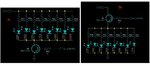
If uses a single NPN transistor to drive LEDs, can anyone tell me what is the advantage and disadvantage to put those LEDs at collector (graph A) or at emitter terminals (graph B)?
Introducing a load in the emitter leg requires you give more attention to the bias. You must raise your bias V so as to turn on the transistor sufficiently.
Therefore your B circuit will require a higher bias than your A circuit. The amount will need to be 2.0 to 2.5 V higher. (I'm assuming 1.8v for red LEDs, plus a few tenths V drop across your current-equalizing resistors.)
This can be done by reducing bias resistor (R80) to 100 ohms. A 3V control pulse will deliver a milliamp or two of bias current.
In comparison the A circuit has a more sensitive bias input which will operate on a lower control voltage. This is an advantage of putting the load in the collector leg.
By the way your equalizing resistors can be as low as 100 ohms per LED (for both A and B circuits). Any oddball LED will still be within a milliamp or two of the others.
This site uses cookies to help personalise content, tailor your experience and to keep you logged in if you register.
By continuing to use this site, you are consenting to our use of cookies.