Continue to Site

Welcome to EDAboard.com

Welcome to our site! EDAboard.com is an international Electronics Discussion Forum focused on EDA software, circuits, schematics, books, theory, papers, asic, pld, 8051, DSP, Network, RF, Analog Design, PCB, Service Manuals... and a whole lot more! To participate you need to register. Registration is free. Click here to register now.

Simple amplifier design

Status
Not open for further replies.

julian403

Full Member level 5
Full Member level 5
Joined
Feb 28, 2014
Messages
254
Helped
1
Reputation
2
Reaction score
1
Trophy points
18
Location
Argentina
Activity points
2,105
What do you think about this ampliffier? yes, I know the power step, class AB, has not polarization (but whit multisim an error occurs if I place the polarization diodes)

amplificador2.PNG

This is the output signal (for me it's allmost rail to rail :shock:)

amplificador.PNG

and this is the bandwidth

amplificador3.PNG


Until now it had never been possible to obtain a great voltage gain to exite the power stage.
But seeing the TL082's schematic I realized that there were current sources. So there I realized that the current source allowed me to have a proper polarization and have a high impedance collector, hoe.
I make it only whit BC548 because it's cheaper and easy to find and for the power stage I'm going to use 2SC5200 and 2SC1943.

The signal distortion I think it's for the software simulations.


And this it's the proteus simulation

Captura2.PNG

Captura23.PNG

amplificadorProteus.PNG

Why the higher the gain less resistance, in the resistances of the polarization of the power stage?
 
Last edited:

Besides missing DC current bias, the circuit has the disadvantage of an output swing far below the supply voltage. Respectively the efficiency is very poor.

Most similar circuits are implementing overall DC feedback for a stable operation point and small output offset.
 

But the output peak voltage signal is 30V and the DC power supply is +-34V
 

The clipped output voltage is +25/-20 V. But did you check the maximal undistorted output voltage?
 
I'm seeing this dessing.

nuevaAmpli1.PNG

Power supply is +/-34

nuevoAmpli2.PNG


What operation point must have transistor Q5? At first Ic is 2 mA without input signal.

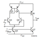
This is the schematic that I took into consideration

____amplificador,_el_de_compensación_en_frecuencia,_necesario_para_que_un[1].gif
 

Hi,

The thread is called "simple amplifier design".
Why not using a monolithic amplifier IC like "TDAxxx" or "LMxxx" ?

Or is it a challenge to build it on your own?

Klaus
 

Hi,

I'd consider changing R1 and Q3 and Q4 for actual current mirrors. Also, I've only simulated a few simple discrete op amp designs, which took a lot of patient fiddling with the current mirrors biasing resistors to get the mix right..., when simulating designs that once you've got the biasing right (i.e. for a voltage follower what goes in is what you should see at the output, give or take a few mV, in the expected range of the input devices/output) it's enlightening to check a good few inputs like stepping the input voltage, trying squarewave, not only sinewave, and trying a few frequencies to see when the op amp loses control and oscillates, when the squarewave begins to degrade unacceptably, and to use a load just under where you see clipping to know how large a load the design will tolerate. 2Hz looks good, maybe 1kHz, 5kHz may show a dismal slew rate...

I think it's okay to expect nothing better than an output 1 Vce below V+ or above V-, if there's only one transistor in line from the respective rail, but with home-brew designs the results may not be quite so good, so input range has to be adapted to the design, not expectations.

It's good to read about op amp design, to understand how, for example, a specific design influences, for example, output resistance (impedance), which will show what load you can get away with, but when designing with discrete components, as opposed to designing the transistors yourself, I don't think it's so easy to relate one method to the other and find it out if you have as little experience as I do.

Measuring/simulating with no load, in my opinion is a bit pointless - you won't see the real voltage swing limitations based on load current, and if you look, a capacitive load (in parallel to a resistive) is often used to evaluate a design.
 
Audio amplifiers are often improving output swing by using one (or two) bootstrap capacitors(s) for the driver stage. It's an effective method if you can live with a lower cut-off frequency for full power output.
 
I'd consider changing R1 and Q3 and Q4 for actual current mirrors
Yes, I just put this with just one transistor to do it fastter but in a good desing as you said it must be a current mirror.
It's good to read about op amp design
Where I can read about it? I means a good reading stuff. For example in all book I had read, like Schilling / Belove I did not find stuff like the build of amp op, just the commun things.

Why not using a monolithic amplifier IC like "TDAxxx" or "LMxxx" ?

Or is it a challenge to build it on your own?

Yes, I have ampliffiers and I had build one whit an LM4780 and class D, but I want to do one of this by myself

- - - Updated - - -

I goes better with this current source, I get 29V max output voltage with a input signal of 1V.

betterone.PNG

betterone2.PNG
 
Last edited:

Hi,

Good for you, glad it's getting even better. A while ago FvM suggested this book to some-one in another post: Gray and Meyer - "Analysis and Design of Analog Integrated Circuits," I also found W Sansen's book - "Analog Design Essentials" well worth reading, people often seem to reference Behzad Razavi's books regarding CMOS op amp design, not sure if they cover BJT circuits. The two books I have read cover op amp design in BJT and MOS really well, I learnt a lot from them. There are loads of other books like this as well. Op Amps for Everyone, by TI, and Op Amp Applications (the book) by Analog Devices, while not per se about op amp design are also very insightful and help with this kind of circuit/project.

What is the goal/main function of the design you're basing this op amp on, please? I'm curious as I've only seen/paid attention to op amps which have current mirrors as the loads for the differential pair, besides the mirror for the tail current. Thanks.
 
The output darlington transistors conduct more when they heat which causes them to conduct more then heat more then conduct more then then heat more .... It is called "thermal runaway".
An audio amplifier or opamp use diodes like you did in one circuit or a transistor to replace the diodes to also conduct when they are heated by the darlingtons to cancel the thermal runaway. They replace your resistor R3.
 
An audio amplifier or opamp use diodes like you did in one circuit or a transistor to replace the diodes to also conduct when they are heated by the darlingtons to cancel the thermal runaway. They replace your resistor R3.
You are rigth, and the diodes will be near the head dissipator.

What is the goal/main function of the design you're basing this op amp on, please? I'm curious as I've only seen/paid attention to op amps which have current mirrors as the loads for the differential pair, besides the mirror for the tail current. Thanks.
Do an ampliffier which can deliver more than 1 ampere. But really what I want is to design it and understand the inner workings. Thanks for the books recommendation! looks nice.
 

by the way, I can do the operational ampliffier, as you can see here

diferential ampliffier.PNG

And the outputs depends of the feedback resistors:

differential ampliffier measure.PNG

differential ampliffier measure3.PNG

but there is just a problem, the voltage offset. I can set it with R3, but there must be difference values for every input output voltage.
 

Hi,

Looking good!

Maybe have a look at Electronics_Ch13 page 13, and Intro2OpAmps page 16, I was unable to find other pdfs with what I mean that showed a full design, perhaps you can incorporate that biasing idea to the circuit you have, with the diodes, etc., and replace R3 by active biasing, I think if biasing it via Itail makes the output too weak, a separate... guess what: current mirror biased at a higher current might help with the voltage offset. If you meant that the output has an offset dependent on input level, that is. I found that at midsupply the output was quite faithful to the input, in fact exactly 550mV or 549.xxxmV in a simulation, but towards either end of the input range drifted by a couple of mV up to about 50mV (I was looking at 1.1V supply simple two or three-stage op amps using the 2N2222A amd 2N2907A) - marginally higher at lower voltages and marginally lower at the high end of the range.
 

Attachments

  • Intro2OpAmps.pdf
    760.8 KB · Views: 105
  • Electronics_Ch13.pdf
    911.1 KB · Views: 132
An opamp (without negative feedback) has a DC gain of hundreds of thousands or millions then it can cancel most of its offset voltage. Your amplifier has an open-loop gain of much less so it cannot cancel much offset.
An opamp has matched transistors so its offset can be low, yours does not.
 
oh thanks! for example in the next example:

Captura.PNG

At what potential must be Vbias to have the max gain and min offset?
 

Hi,

Honest answer: I don't know, I found out by experimentation, and only focussed on the resistor value/bias current that made Vout = Vin. The books explain general biasing and specific biasing for analysed designs. An engineer could tell you the actual ratios that work. If I remember well, two-stage op amps such as the one in the last post seem to use the same bias as used for Itail, which I think is supposed to be twice the value of Ic Q1 and Ic Q2, ...but with a separate bias of higher current value it should have a better Iout ability. I wouldn't value my observations too much, 'though.
 
Your last amplifier operates in class-A. Most audio amplifiers and opamps operate in class-AB.
Your Q6 has a fairly low output impedance and its gain is affected by the load impedance. It pulls up with plenty of power.
Your Q7 is a high impedance current source with no input or output signal and has a weak pull down current.
 
At what potential must be Vbias to have the max gain and min offset?

In general, make resistance small in the emitter leg, to get maximum gain (or max sensitivity). The long-tail pair works in a non-obvious manner. As you turn on Q1, it tends to turn off Q2 (and vice-versa). There are several adjustments you can make, to center the range of output, to increase or decrease gain, to get matching response from Q1 & Q2, etc.

As you adjust one transistor's response, it changes action elsewhere in the long-tail pair.
As you change Vee, it reduces or increases output voltage. This can be used as a way to adjust offset voltage.
It becomes apparent that there's a lot going on here.

I have experimented with simulations of a simple differential amplifier. I use only Q1, Q2, variable Vee, and fixed resistor at the bottom of the long-tail pair. I find I need to make a minimal parts count, in order to figure out what affects what. Someday my mind may get a grasp of the operation of a differential amplifier.
8-O
 

Status
Not open for further replies.

Similar threads

Part and Inventory Search

Welcome to EDABoard.com

Sponsor

Back
Top